Straining the memory: Prototype strain engineered materials are the future of data storage
- Sep 20, 2017
- 2 min read

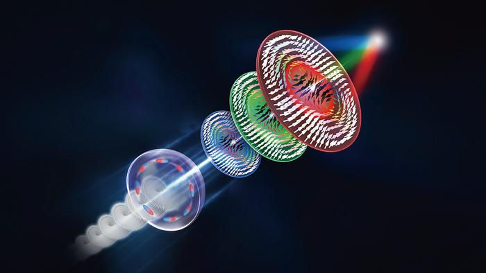
Researchers from the Singapore University of Technology and Design (SUTD) and Shanghai Institute of Microsystems and Information Technology have nano-engineered a superlattice data storage material. Data is recorded at the interfaces of the superlattice layers. When the atoms at the interface are disordered, the material has a high electrical resistance while the ordered interface has a low electrical resistance.
Since only the interface switches, a subset of layers within the material can remain unchanged and crystalline. This means that the interface can be engineered by the non-switching layers - the entire structure need not switch into a disordered state. This makes the superlattice very different to unstructured phase change memory alloys, such as the Ge2Sb2Te5 alloy.
The authors showed in a paper published in Nano Futures that fast switching in these nanostructured materials is due to avalanche atomic switching at the interface. The first atom that switches requires a large amount of energy, but subsequent atoms require less energy. As more atoms switch, the energy required for subsequent atoms to switch is lowered. This leads to an exponential increase in the switching probability with the number of atoms switching.
Zhou et al showed that the energy for the first atom to switch can be engineered by straining the layer interfaces. The research team created prototype memory devices, which exploit this effect that outperformed state-of-the-art phase change memory devices. The switching voltage, current, and switching time are substantially reduced while the electrical resistance changes by a factor of 500. Thus these prototype devices are faster and more efficient than current competing technologies.
One of the members of the research team, Assistant Professor Robert Simpson, said: "The superlattices devices are remarkably energy efficient. We foresee this technology impacting new 3D memory architectures, such as Intel's 3D x-point. We are now building on the success of these data storage materials by optimising similar phase change materials for switchable nano photonics applications."
Avalanche atomic switching in strain engineered Sb2Te3–GeTe interfacial phase-change memory cells Xilin Zhou, Jitendra K Behera, Shilong Lv, Liangcai Wu, Zhitang Song and Robert E Simpson http://dx.doi.org/10.1088/2399-1984/aa8434


Comments