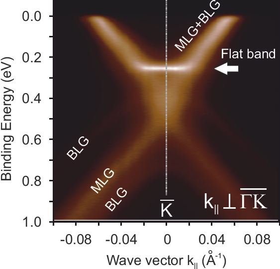
Scientists at HZB have found evidence that double layers of graphene have a property that may let them conduct current completely without resistance. They probed the bandstructure at BESSY II with extremely high resolution ARPES and could identify a flat area at a surprising location.
Carbon atoms have diverse possibilities to form bonds. Pure carbon can therefore occur in many forms, as diamond, graphite, as nanotubes, football molecules or as a honeycomb-net with hexagonal meshes, graphene. This exotic, strictly two-dimensional material conducts electricity excellently, but is not a superconductor. But perhaps this can be changed.
A complicated option for superconductivity
In April 2018, a group at MIT, USA, showed that it is possible to generate a form of superconductivity in a system of two layers of graphene under very specific conditions: To do this, the two hexagonal nets must be twisted against each other by exactly the magic angle of 1.1°. Under this condition a flat band forms in the electronic structure. The preparation of samples from two layers of graphene with such an exactly adjusted twist is complex, and not suitable for mass production. Nevertheless, the study has attracted a lot of attention among experts.
The simple way to flat bands
But there is one more, much simpler way of flat band formation. This was shown by a group at the HZB around Prof. Oliver Rader and Dr. Andrei Varykhalov with investigations at BESSY II. The samples were provided by Prof. Thomas Seyller, TU Chemnitz. There they are produced using a process that is also suitable for the production of larger areas and in large quantities: A silicon carbide crystal is heated until silicon atoms evaporate from the surface, leaving first a single-layer of graphene on the surface, and then a second layer of graphene. The two graphene layers are not twisted against each other, but lie exactly on top of each other.
Scanning the band structure with ARPES
At BESSY II, the physicists are able to scan the so-called band structure of the sample. This band structure provides information on how the charge carriers are distributed among the quantum-mechanically permitted states and which charge carriers are available for transport at all. The angle-resolved photoemission spectroscopy (ARPES) at BESSY II enables such measurements with extremely high resolution.
An interesting region under scrutiny
Via an exact analysis of the band structure, they identified an area that had previously been overlooked. "The double layer of graphene has been studied before because it is a semiconductor with a band gap," explains Varykhalov. "But on the ARPES instrument at BESSY II, the resolution is high enough to recognize the flat area next to this band gap.”
"It is an overseen property of a well-studied system”, first author Dr. Dmitry Marchenko points out: “It was previously unknown that there is a flat area in the band structure in such a simple well-known system."
Superconductivity? Needs still a little help
This flat area is a prerequisite for superconductivity but only if it is situated exactly at the so-called Fermi energy. In the case of the two-layer graphene, its energy level is only 200 milli-electron volts below the Fermi energy, but it is possible to raise the energy level of the flat area to the Fermi energy either by doping with foreign atoms or by applying an external voltage, the so-called gate voltage.
The physicists have found that the interactions between the two graphene layers and between graphene and the silicon carbide lattice are jointly responsible for the formation of the flat band area. "We can predict this behavior with very few parameters and could use this mechanism to control the band structure," adds Oliver Rader.
Published in Science Advances (2018): Extremely Flat Band in Bilayer Graphene; D. Marchenko, D. V. Evtushinsky, E. Golias, A. Varykhalov, Th. Seyller and O. Rader
DOI: 10.1126/sciadv.aau0059
HZB
#Graphene #Superconductivity #Nanotubes #Semiconductors

Waste polyamide-derived CQDs show continuous photoluminescence tuning from 308 to 552 nm through sequential defect-state engineering, with optical transition energies decreasing from 4.32 to 2.50 eV. @Christian Ebere Enyoh from Saitama University Carbon quantum dots (CQDs) are fluorescent carbon nanomaterials with potential applications in sensing, optoelectronics, displays, anti-counterfeiting, and environmental technologies. Their optical properties can be adjusted by modifying the carbon...

The researchers used circularly polarized light at normal incidence and found that helicity-dependent photocurrents appeared perpendicular to the crystal’s polarization but vanished when measured parallel to it, supporting a bulk origin of CPGE. @Institute of Science Tokyo The circular photogalvanic effect (CPGE), a phenomenon that generates helicity-dependent photocurrents in noncentrosymmetric materials, can originate purely from a crystal's internal structure without contribution from the...

Summary of gold nanoparticle growth programming in liposome based on localization of biomineralization peptide The position of biomineralization peptides within liposomes can influence how gold nanoparticles grow, reports a research team from Institute of Science Tokyo. Peptides localized at the membrane interface promote branched structures, while those confined to the liposome interior favor spherical nanoparticles. The findings offer a new strategy for controlling nanoscale reaction...
