University of Basel
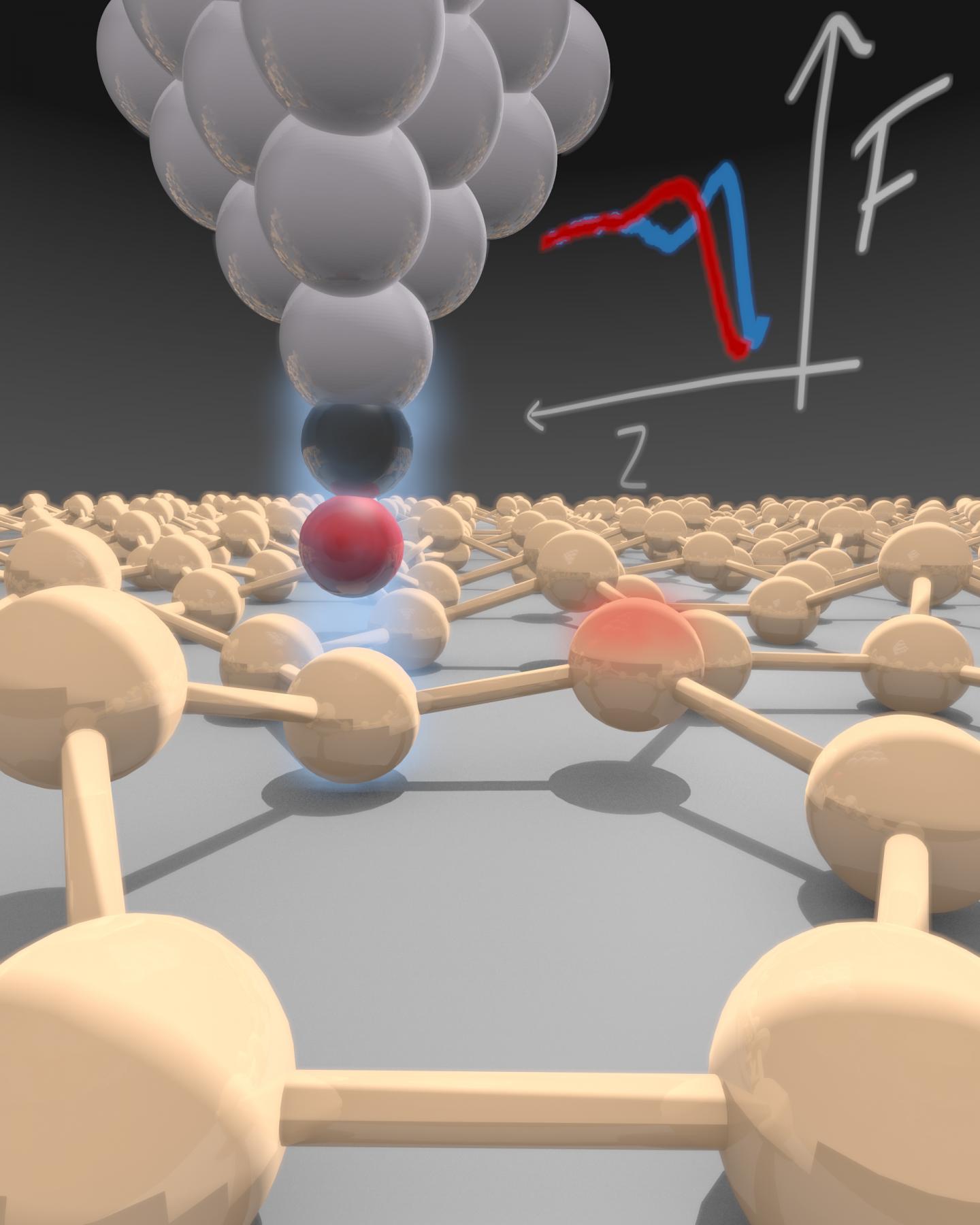
Silicene consists of a single layer of silicon atoms. In contrast to the ultra-flat material graphene, which is made of carbon, silicene shows surface irregularities that influence its electronic properties. Now, physicists from the University of Basel have been able to precisely determine this corrugated structure. As they report in the journal PNAS, their method is also suitable for analyzing other two-dimensional materials.
Since the experimental production of graphene, two-dimensional materials have been at the heart of materials research. Similar to carbon, a single layer of honeycombed atoms can be made from silicon. This material, known as silicene, has an atomic roughness, in contrast to graphene, since some atoms are at a higher level than others.
Silicene not completely flat
Now, the research team, led by Professor Ernst Meyer of the Department of Physics and the Swiss Nanoscience Institute of the University of Basel, has succeeded in quantitatively representing these tiny height differences and detecting the different arrangement of atoms moving in a range of less than one angstrom - that is, less than a 10-millionth of a millimeter.
"We use low-temperature atomic force microscopy with a carbon monoxide tip," explains Dr. Rémy Pawlak, who played a leading role in the experiments. Force spectroscopy allows the quantitative determination of forces between the sample and the tip. Thus, the height in relation to the surface can be detected and individual atoms can be chemically identified. The measurements show excellent agreement with simulations carried out by partners at the Instituto de Ciencia de Materiales de Madrid (ICMM).
Different electronic properties
This unevenness, known as buckling, influences the electronic properties of the material. Unlike graphene, which is known to be an excellent conductor, on a silver surface silicene behaves more like a semiconductor. "In silicene, the perfect honeycomb structure is disrupted. This is not necessarily a disadvantage, as it could lead to the emergence of interesting quantum phenomena, such as the quantum spin hall effect," says Meyer.
The method developed by the researchers in Basel offers new insights into the world of two-dimensional materials and the relationship between structure and electronic properties.
Quantitative determination of atomic buckling of silicene by atomic force microscopy
Rémy Pawlak, Carl Drechsel, Philipp D’Astolfo, Marcin Kisiel, Ernst Meyer, and Jorge Iribas Cerda
PNAS (2019)
Contact information:
Ernst Meyer
Professor of Experimental Physics
ernst.meyer@unibas.ch
Phone: +41 (0)61 207 37 24
Meyer Group - Nanolino Lab
