Japan Science and Technology Agency (JST)
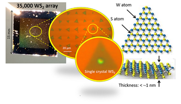
In Japan Science and Technology Agency's Strategic Basic Research Programs, Associate Professor Toshiaki Kato and Professor Toshiro Kaneko of the Department of Electronic Engineering, Graduate School of Engineering, Tohoku University succeeded in clarifying a new synthesis mechanism regarding transition metal dichalcogenides (TMD)1), which are semiconductor atomic sheets having thickness in atomic order.
Because it is difficult to directly observe the aspect of the growing process of TMD in a special environment, the initial growth process remained unclear, and it has been desirable to elucidate a detailed mechanism of synthesis to obtain high-quality TMD.
An in-situ observing synthesis method2) has been developed by our research group to examine the growth aspect of TMD as a real-time optical image in a special high temperature atmosphere of about 800°C in the presence of corrosive gases. In addition, a synthesis substrate, which is a mechanism to control diffusion during the crystal growth of a precursor3), has been developed in advance; further, it has been clarified that the growing precursor diffuses a distance about 100 times larger than in conventional semiconductor materials. It was also demonstrated that nucleation occurs due to the involvement of the precursor in a droplet state. Furthermore, by utilizing this method, a large-scale integration of more than 35,000 monolayer single crystal atomic sheets has been achieved on a substrate in a practical scale (Figure 1).
Utilizing the results of the present research, the large-scale integration of atomic-order thick4) semiconductor atomic sheets can be fabricated and is expected to be put into practical use in the field of next-generation flexible electronics.
Notes
1) Transition Metal Dichalcogenides: TMD
Atomic layer materials are similar to graphene. This material has a structure in which a transition metal is sandwiched between the chalcogen atoms. Graphene shows metallic conduction characteristics but TMD has a band gap to show semiconductor properties and is expected to be applied in the field of semiconductor devices.
2) In-situ monitoring synthesis method
A crystal growing technique capable of monitoring the synthesis states in real time.
3) Precursor
Raw material for crystal growing. When incorporated into the crystal, a part or all of it becomes an element constituting the crystal.
4) Atomic order
The size of one atom is about several angstroms (one angstrom is one ten billionth of a meter). This means the size of one to several integrated atoms.
Nucleation dynamics of single crystal WS2 from droplet precursors uncovered by in-situ monitoring
Chao Li, Tomoya Kameyama, Tomoyuki Takahashi, Toshiro Kaneko & Toshiaki Kato
Scientific Reports volume 9, Article number: 12958 (2019)
DOI: 10.1038/s41598-019-49113-0
Contat information:
Toshiaki Kato
Associate Professor at Department of Electronic Engineering, Tohoku University
kato12ecei.tohoku.ac.jp
Phone: +81-22-795-7046
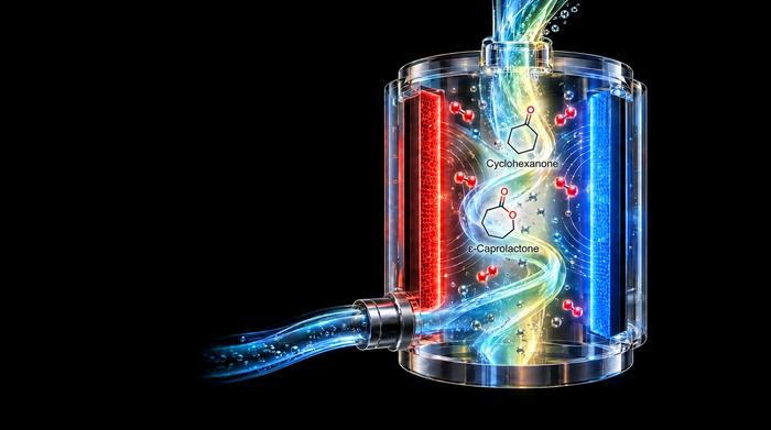
Researchers led by Professor Jaeyune Ryu at Seoul National University identified local pH near electrodes as a decisive variable in organic electrosynthesis. By designing a reactor that narrows electrode spacing and flows electrolyte to counterbalance acidic and alkaline zones, they raised selectivity for lactones and epoxides, feedstocks for biodegradable plastics, polyurethanes, adhesives, and epoxy resins, from about 16% to 97% using only oxygen and electricity, eliminating added peroxide…
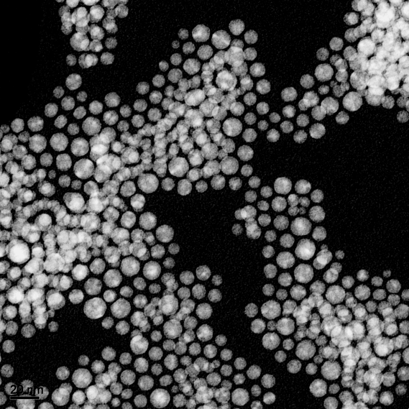
Silver nanoparticles with diameters of ~10 nm deliver the best performance as electrocatalysts. The silver particles are sprayed onto the electrode together with a conductive carbon powder. The ideal mixture consists of 20 per cent by mass silver and 80 per cent by mass carbon powder. This image was taken using a transmission electron microscope (TEM). © HZB Via electrolysis, CO₂ can be reduced to CO, a raw material for further chemical products such as fuels. Within the GreenQuest Project,...
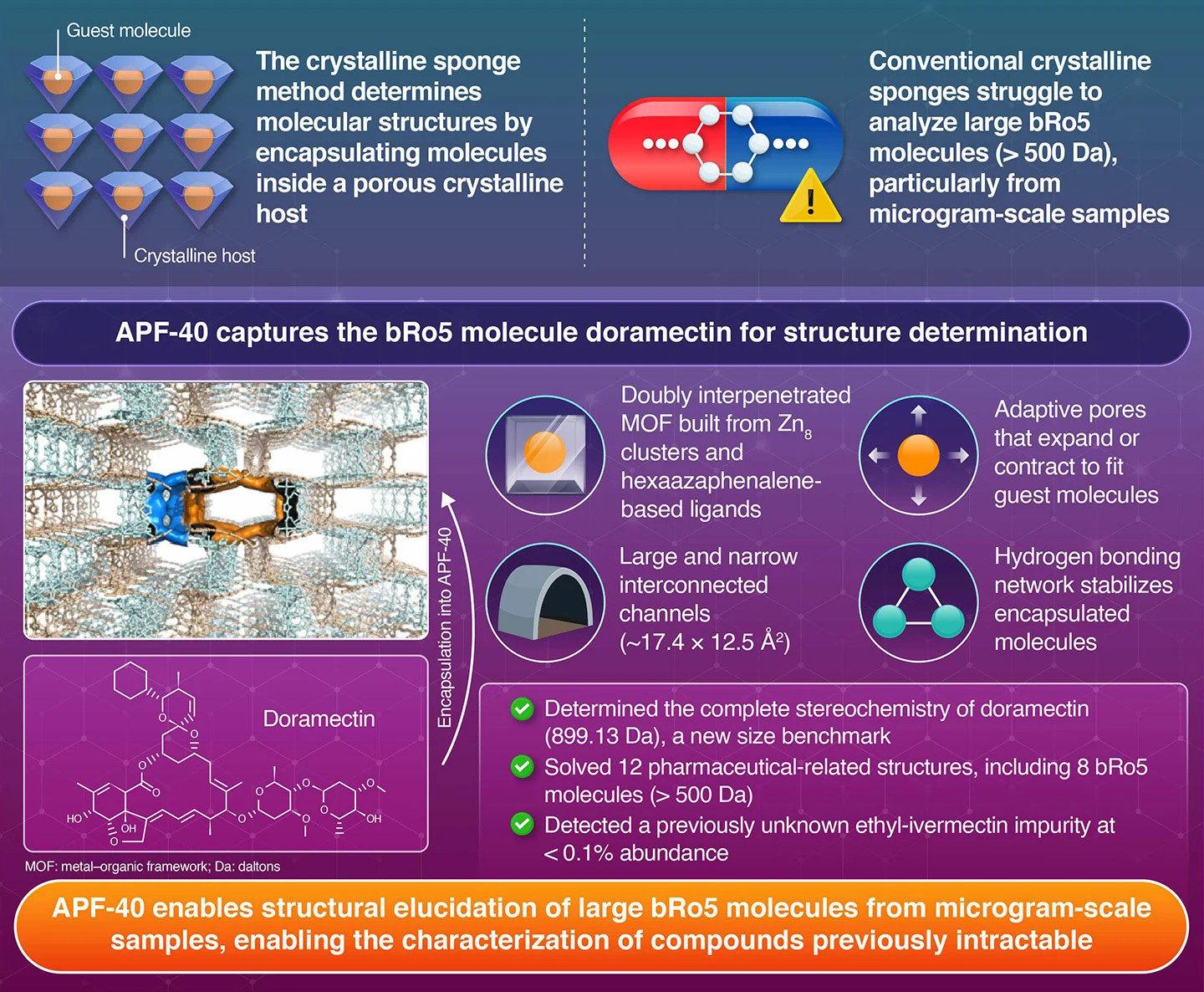
A flexible metal–organic framework developed by researchers from Institute of Science Tokyo enables the structural determination of large "beyond rule of 5" molecules from microgram-scale samples. Using APF-40 as a crystalline sponge, the researchers determined the structures of 12 pharmaceutical-related molecules, including the 899 Da drug molecule doramectin and trace ivermectin derivatives. The method could aid drug discovery, natural products research, and the characterization of rare...