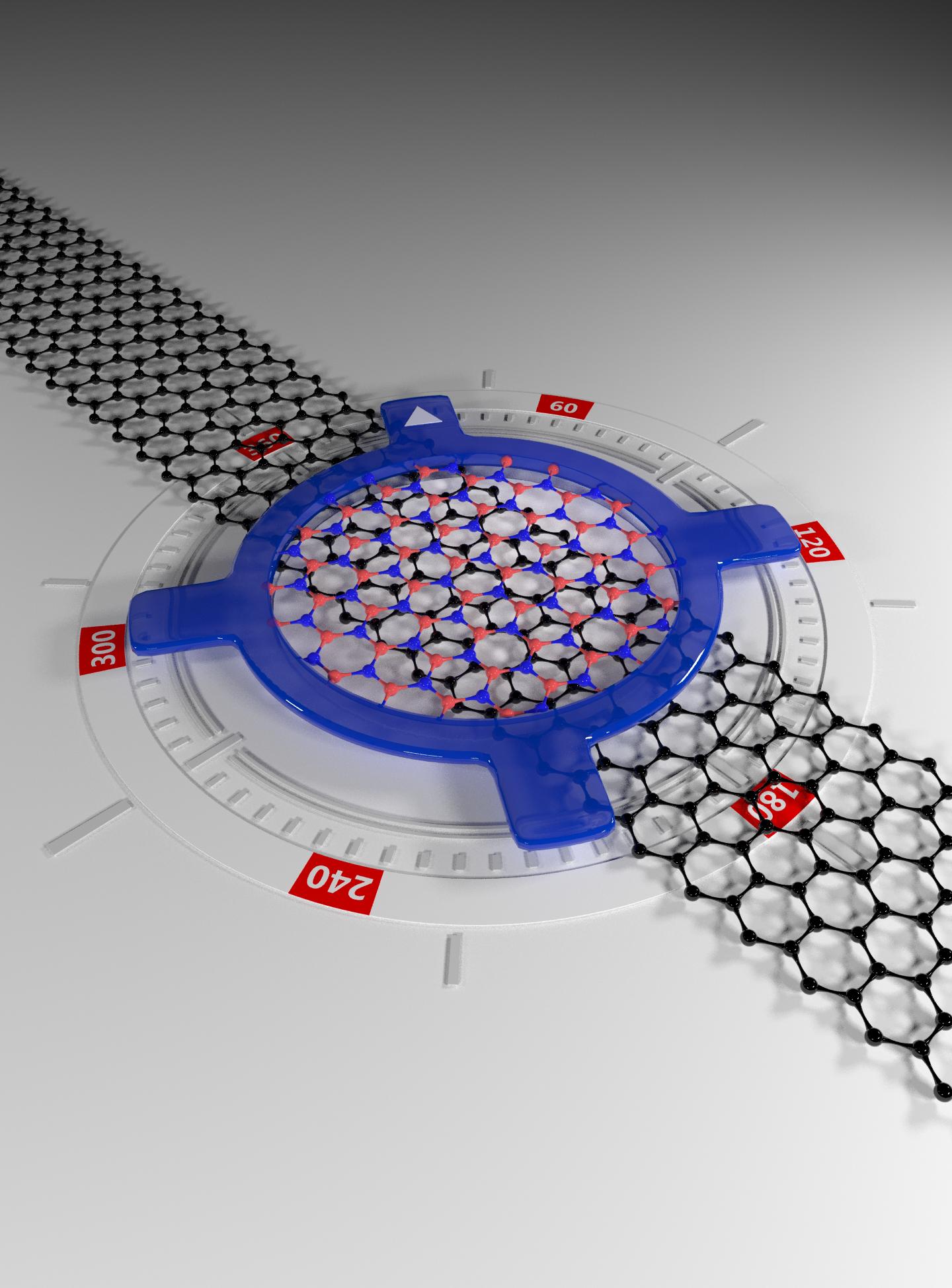
Two-dimensional (2D) materials such as graphene have unique electronic, magnetic, optical, and mechanical properties that promise to drive innovation in areas from electronics to energy to materials to medicine. Columbia University researchers report a major advance that may revolutionize the field, a "twistronic" device whose characteristics can be varied by simply varying the angle between two different 2D layers placed on top of one another.
In a paper published online today in Science, the team demonstrates a novel device structure that not only gives them unprecedented control over the angular orientation in twisted-layer devices, but also allows them to vary this angle in situ, so that the effects of twist angle on electronic, optical, and mechanical properties can be studied in a single device.
Led by Cory Dean (physics, Columbia University) and James Hone (mechanical engineering, Columbia Engineering), the team built upon techniques that they previously pioneered to mechanically layer graphene and other 2D materials, one on top of another, to form new structures. "This mechanical assembly process allows us to mix and match different crystals to construct entirely new materials, often with properties fundamentally different from the constituent layers," says Hone, leader of Columbia's Materials Research Science and Engineering Center (MRSEC), which investigates the properties of these heterostructures. "With hundreds of 2D materials available, the design possibilities are enormous."
Recent studies have shown that rotational alignment between the layers plays a critically important role in determining the new properties that arise when materials are combined. For example, when conducting graphene is placed on top of insulating boron nitride with the crystal lattices perfectly aligned, graphene develops a band gap. At non-zero angles, the band gap disappears and intrinsic graphene properties are recovered. Just this past March, researchers at MIT reported the groundbreaking discovery that two stacked layers of graphene can exhibit exotic properties including superconductivity when the twist angle between them is set to 1.1 degrees, referred to as the "magic angle."
In previous approaches to fabricating structures with rotationally misaligned layers, the angle was set during the assembly process. This meant that once the device was made, its properties were fixed. "We were finding this approach frustrating, since very small errors in alignment could give entirely different results," says Dean. "It would be great to make a device in which we could study its properties while continuously rotating its layers and so the question was, how to do this?"
The answer, the Columbia researchers realized, was to take advantage of the low friction that exists at the interface between the layers, which are held together by van der Waals forces that are much weaker than the atomic bonds within each layer. This low friction?which makes 2D materials very good as solid lubricants?makes controlled assembly at a desired angle very difficult. The Columbia group used the low friction characteristic to their advantage by designing a device structure in which, instead of preventing rotation, they could intentionally and controllably vary the rotation angle.
The team used graphene/boron-nitride heterostructures to demonstrate the reach of their technique. In these structures, when the layers are not crystallographically aligned, the materials preserve their original properties (e.g., graphene will have a semi-metallic character) but when the layers are aligned, the properties of graphene change, opening an energy gap and behaving as a semiconductor. The researchers showed that this fine-tuning of the heterostructure's properties affects its optical, mechanical, and electronic responses.
"Notably, we demonstrated that the energy gap observed in graphene is tunable and can be turned on or off on demand just by changing the orientation between the layers," says Rebeca Ribeiro, who led this work as a post-doctoral researcher at Columbia and is now a CNRS research scientist at the French Center for Nanoscience and Nanotechnology (C2N-CNRS). "The tuning of this energy gap not only represents a major step toward the future use of graphene in varied applications, but also provides a general demonstration in which the device properties of 2D materials are dramatically varied with rotation ".
From a technological point of view, the ability to tune the properties of a layered material by varying the twist angle provides the possibility for a single material platform to perform a variety of functions. For example, electronic circuits are built from a finite number of components including metallic conductors, insulators, semiconductors, and magnetic materials. This process requires integration of a variety of different materials and can pose a significant engineering challenge. In contrast, a single material that can be locally "twisted" to realize each of these components could enable significant new engineering opportunities.
In addition, the ability to dynamically tune a system with mechanical twisting offers a new switching capability that could enable entirely new device applications. For example, traditional switches typically vary between two well-defined states (on or off, magnetic or not, etc.). The Columbia platform could enable the possibility to switch between an arbitrary number of complementary states.
Dean and Hone are now using their new technique to study other combinations of 2D materials in which the properties can be tuned by angular alignment. They are looking particularly at the recent discovery of superconductivity in twisted bilayer graphene and exploring whether it may be a general feature of twisted bilayers made from arbitrary 2D materials.
Dean adds, "Our study demonstrates a new degree of freedom, namely rotational orientation between layers, that just doesn't exist in conventional semiconductor heterostructures. This is a rare occasion in the semiconductor field where we are truly forging a new path, and opens the door to a whole new field of research where material properties can be varied simply by twisting the structure."
Twistable electronics with dynamically rotatable heterostructures
Rebeca Ribeiro-Palau, Changjian Zhang, Kenji Watanabe, Takashi Taniguchi, James Hone, Cory R. Dean
Science 17 Aug 2018: Vol. 361, Issue 6403, pp. 690-693
DOI: 10.1126/science.aat6981
Contact information:
Cory Dean
Columbia University's Dept of Physics
cd2478@columbia.edu
Tel: (212) 854-3189
Webpage: http://www.deanlab.com/
James Hone
Columbia University's Dept of Mechanical Engineering
jh2228@columbia.edu
Tel: (212) 854-6244
Fax: (212) 854-3304
Webpage: http://hone.me.columbia.edu/
Columbia University's Fu Foundation School of Engineering and Applied Science
#Graphene #2DMaterials #Nanostructures

Waste polyamide-derived CQDs show continuous photoluminescence tuning from 308 to 552 nm through sequential defect-state engineering, with optical transition energies decreasing from 4.32 to 2.50 eV. @Christian Ebere Enyoh from Saitama University Carbon quantum dots (CQDs) are fluorescent carbon nanomaterials with potential applications in sensing, optoelectronics, displays, anti-counterfeiting, and environmental technologies. Their optical properties can be adjusted by modifying the carbon...

The researchers used circularly polarized light at normal incidence and found that helicity-dependent photocurrents appeared perpendicular to the crystal’s polarization but vanished when measured parallel to it, supporting a bulk origin of CPGE. @Institute of Science Tokyo The circular photogalvanic effect (CPGE), a phenomenon that generates helicity-dependent photocurrents in noncentrosymmetric materials, can originate purely from a crystal's internal structure without contribution from the...

Summary of gold nanoparticle growth programming in liposome based on localization of biomineralization peptide The position of biomineralization peptides within liposomes can influence how gold nanoparticles grow, reports a research team from Institute of Science Tokyo. Peptides localized at the membrane interface promote branched structures, while those confined to the liposome interior favor spherical nanoparticles. The findings offer a new strategy for controlling nanoscale reaction...