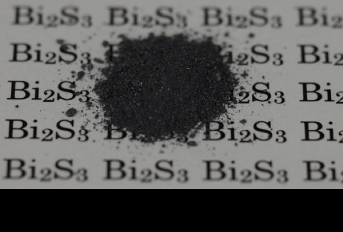
Developing materials suitable for use in optoelectronic devices is currently a very active area of research. The search for materials for use in photoelectric conversion elements has to be carried out in parallel with developing the optimal film formation process for each material, and this can take a few years for just one material. Until now there has been a trade-off, balancing electronic properties and material morphology. Researchers at Osaka University have developed a two-step process that can produce materials with good morphological properties in addition to excellent photoresistor performance. Their findings were published in the Journal of Physical Chemistry Letters.
Bismuth sulfide, Bi2S3, belongs to a class of materials known as metal chalcogenides, which show significant promise owing to their optical and electronic properties. However, the performance of Bi2S3-based photoresponsive devices is dependent on the method used to process the film, and many of the reported approaches are hampered by low film crystallinity. Even when high crystallinity is achieved, the nature of the grains can have a negative effect on performance, therefore films with low surface roughness and large grain size are desirable.
"We searched more than 200 materials using a unique, ultra high-speed screening method that can evaluate performance, even when only powdered samples are available," study corresponding author Akinori Saeki says. "We found that bismuth sulfide, which is inexpensive and less toxic than conventional inorganic solar cell materials, can be processed in a way that does not compromise its excellent photoelectrical properties."
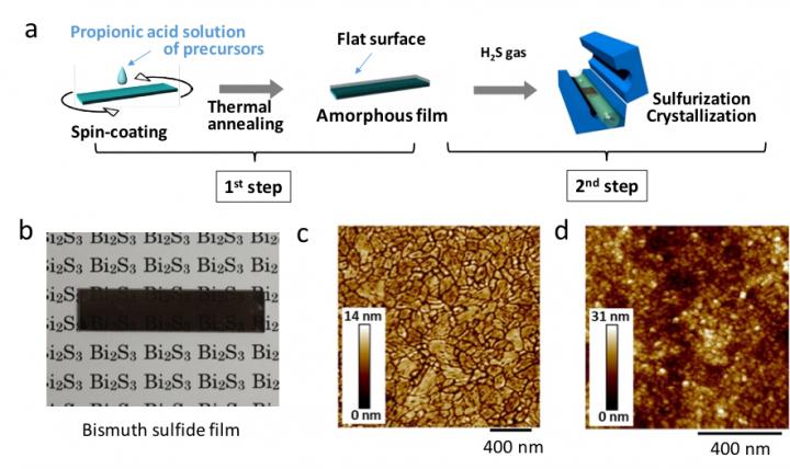
The technique used produces a 2D layered film in two treatment steps; solution spin-coating followed by crystallization. The photo response performance of the resulting film showed improvements of 6-100 times compared with those of films prepared using other processing methods. Owing to the non-toxic and abundant nature of bismuth and sulfur, the findings are expected to influence the development of commercial optoelectronic devices including solar cells.
"We demonstrated a facile processing technique that does not compromise material performance," lead author Ryosuke Nishikubo says. "We believe that solution-processable bismuth-based semiconductors are viable alternatives to commercially available inorganic solar cells and show promise for widespread future use. The fact that they are non-toxic also sets them apart from other alternative optoelectronic materials, such as lead halide perovskites."
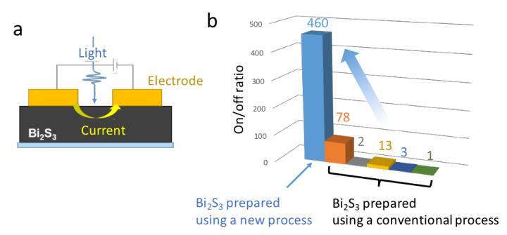
Processing materials for device applications without compromising their electronic properties is important for making materials commercially relevant. The reported process has been used to successfully prepare other metal sulfide semiconductors such as lead sulfide, demonstrating the versatility of the approach.
The article, "Solution-Processed Bi2S3 Photoresistor Film To Mitigate a Trade-off between Morphology and Electronic Properties" was published in the Journal of Physical Chemistry Letters, https://doi.org/10.1021/acs.jpclett.8b02218.
Osaka University
#Optoelectronic #Nanoelectronics #MaterialScience #Semiconductors
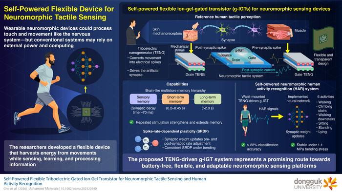
The proposed TENG-driven g-IGT is a flexible, self-powered neuromorphic device capable of reproducing multiple memory states and spike-rate-dependent learning Neuromorphic devices, which are designed to emulate aspects of biological neural networks, are promising candidates for developing low-power and intelligent sensing technologies, including wearable applications. Among the device architectures explored for neuromorphic computing, graphene-channel ion-gel-gated transistors (g-IGTs) are...

Rice University researchers have shown that sub-nanometer wrinkles in graphene generate flexoelectric charge separation, reshaping local electrical behavior through curvature alone. Extreme bending produces polarization far stronger than in larger systems and may enable geometry-controlled electronics without chemical doping. Published in Advanced Materials.

Researchers at NC State have extended twistronics beyond van der Waals materials into strongly bonded crystalline oxides. By stacking sodium niobate membranes with twist angles controlled down to 0.1 degrees, and confirming results via synchrotron X-ray diffraction, the team found interlayer bonds distort the atomic lattice, shifting phase structure and domain configuration. The technique works at near-millimeter scale, far larger than typical twistronic devices, marking a real step toward pract