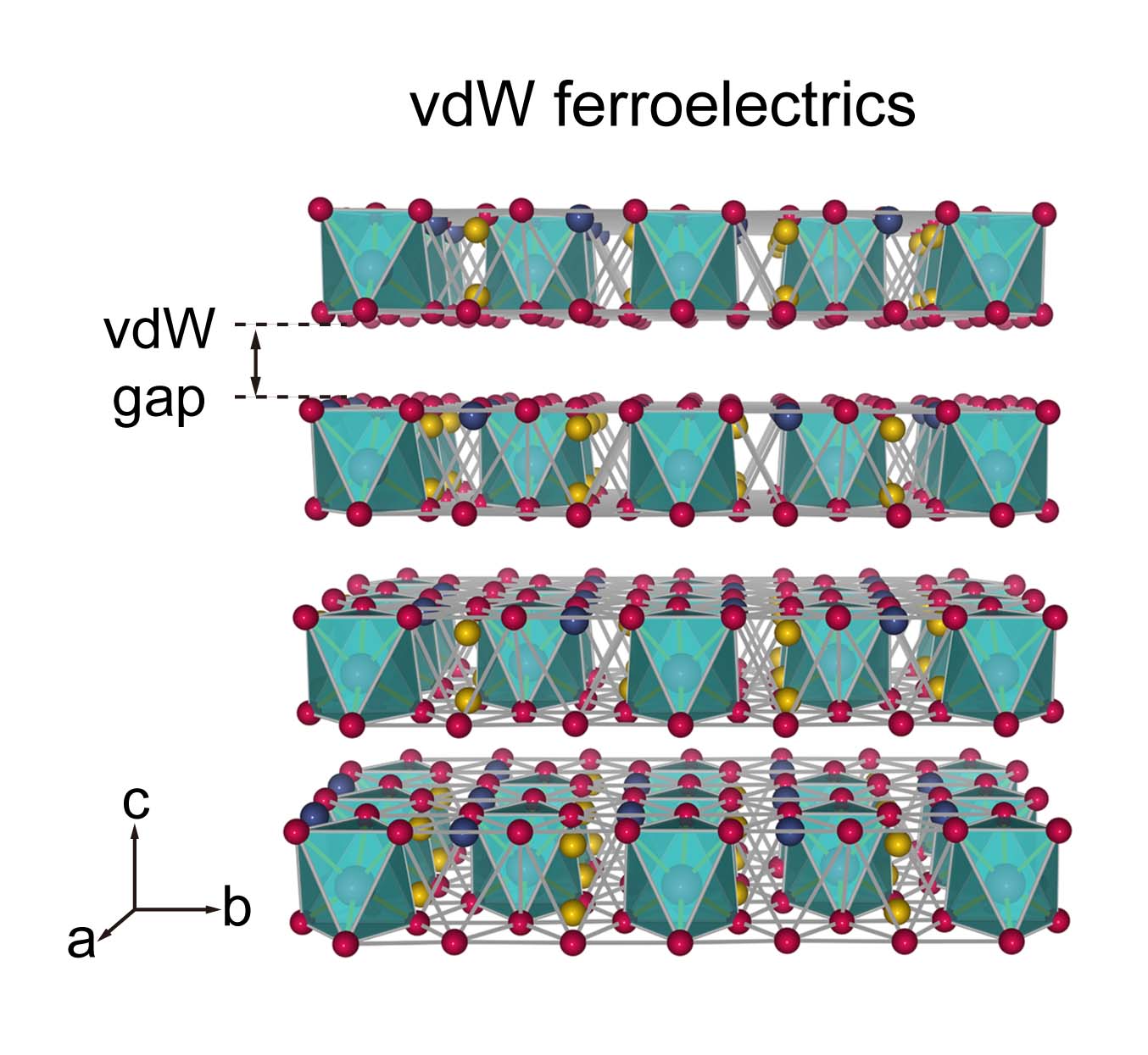
A UNSW paper published recently in Nature Reviews Materials presents an exciting overview of the emerging field of 2D ferroelectric materials with layered van-der-Waals crystal structures: a novel class of low-dimensional materials that is highly interesting for future nanoelectronics.
Future applications include ultra-low energy electronics, high-performance, non-volatile data-storage, high-response optoelectronics, and flexible (energy-harvesting or wearable) electronics.
Structurally different from conventional oxide ferroelectrics with rigid lattices, van der Waals (vdW) ferroelectrics have stable layered structures with a combination of strong intralayer and weak interlayer forces (see figure).
These special atomic arrangements, in combination with the ferroelectric order, give rise to fundamentally new phenomena and functionalities not found in conventional materials.
“Fundamentally new properties are found when these materials are exfoliated down to atomically thin layers,” says author Dr Dawei Zhang. “For example, the origin of the polarization and the switching mechanisms for the polar order can be different from conventional ferroelectrics, enabling new material functionality.”
One of these material’s most intriguing aspects is their easily stackable nature because of the weak van-der-Waals interlayer bonds, which means that vdW ferroelectrics are readily integrable with highly dissimilar crystal-structure materials, such as industrial silicon substrates, without interfacial issues.
“This makes them highly attractive as building blocks for post-Moore’s law electronics,” says author Prof Jan Seidel, also at UNSW.
From the perspective of applications and novel functionalities, vdW ferroelectrics present a wide range of opportunities for nanoelectronics owing to their easily obtainable ferroelectricity at the nanoscale, and dangling bonds-free, clean vdW interfaces that facilitate CMOS-compatible (current silicon technology) integration.
The new review discusses experimentally verified vdW ferroelectric systems and their unique characteristics, such as quadruple-well potentials, metallic ferroelectricity and dipole-locking effects. It also discusses engineered vdW ferroelectricity in stacks of otherwise nonpolar parent materials created by artificially breaking centrosymmetry.
Additionally, innovative device applications harnessing vdW ferroelectricity are showcased, including electronic transistors able to beat the fundamental thermodynamic limits, non-volatile memories and optoelectronic and flexible devices. Recent progress and existing challenges provide a perspective on future research directions and applications.
“It’s a relatively new field, so there are still many challenges that need to be solved to realize the full technological potential of these materials,” says author Dr Pankaj Sharma. “For example, we need to address large-area, uniform, wafer scale growth, and integration methods. These will allow development of futuristic low-energy electronics and computing solutions.”
Given the recent emergence of vdW ferroelectrics, the materials library of such systems is quickly evolving. This leaves room for new developments, such as multiferroicity and coupled functionalities of multiple orders, for example ferroelectricity and magnetism, and the functionality of domain walls in such materials.
Reference
Ferroelectric order in van der Waals layered materials
Dawei Zhang, Peggy Schoenherr, Pankaj Sharma & Jan Seidel

Waste polyamide-derived CQDs show continuous photoluminescence tuning from 308 to 552 nm through sequential defect-state engineering, with optical transition energies decreasing from 4.32 to 2.50 eV. @Christian Ebere Enyoh from Saitama University Carbon quantum dots (CQDs) are fluorescent carbon nanomaterials with potential applications in sensing, optoelectronics, displays, anti-counterfeiting, and environmental technologies. Their optical properties can be adjusted by modifying the carbon...

The researchers used circularly polarized light at normal incidence and found that helicity-dependent photocurrents appeared perpendicular to the crystal’s polarization but vanished when measured parallel to it, supporting a bulk origin of CPGE. @Institute of Science Tokyo The circular photogalvanic effect (CPGE), a phenomenon that generates helicity-dependent photocurrents in noncentrosymmetric materials, can originate purely from a crystal's internal structure without contribution from the...

Summary of gold nanoparticle growth programming in liposome based on localization of biomineralization peptide The position of biomineralization peptides within liposomes can influence how gold nanoparticles grow, reports a research team from Institute of Science Tokyo. Peptides localized at the membrane interface promote branched structures, while those confined to the liposome interior favor spherical nanoparticles. The findings offer a new strategy for controlling nanoscale reaction...
