Lund, 1 October 2026. AlixLabs AB, a Swedish semiconductor equipment company developing Atomic Layer Etch Pitch Splitting (APS™), has started a six-month evaluation project to assess the potential of its APS™ technology for advanced semiconductor patterning within the NanoIC pilot line, coordinated by imec.
The project will evaluate the technology in an advanced pilot manufacturing environment. It will combine AlixLabs' atomic layer etch-based pitch splitting process with imec's advanced lithography, process integration and metrology capabilities, made available through the infrastructure of the NanoIC pilot line.
APS™ is a pitch-splitting process in which pre-patterned structures are selectively divided to create two lines from one original feature, doubling pattern density. The process uses atomic layer etching to provide highly controlled material removal and is intended to reduce the number of process steps compared with conventional multiple-patterning approaches such as litho-etch-litho-etch, self-aligned double patterning and self-aligned quadruple patterning.
For the evaluation, imec will prepare line-and-space structures with feature sizes comparable to some of the most advanced semiconductor processes in production today. The structures will be characterized before being sent to AlixLabs for APS™ process development. AlixLabs will initially develop and assess the process on coupons before transferring selected process conditions to full wafers.
"This evaluation gives AlixLabs the opportunity to assess APS TM in a highly relevant and rigorous semiconductor pilot line environment," said Jonas Sundqvist, CEO of AlixLabs. "The strategic value for us is the ability to generate data using imec's established expertise, metrology and process methodology."
Source: AlixLabs AB news
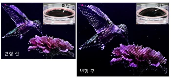
A joint team has created the first ultra-high-resolution stretchable quantum dot display that keeps its image sharp while stretching like skin. By chemically bonding quantum dots to an elastic polymer and stamping fine patterns via a new LIFT process, they reached 16,000 pixels per inch and 53,300 nits, far surpassing earlier stretchable devices, with stable operation at 65% elongation. The advance could accelerate commercial wearable displays and electronic skin.
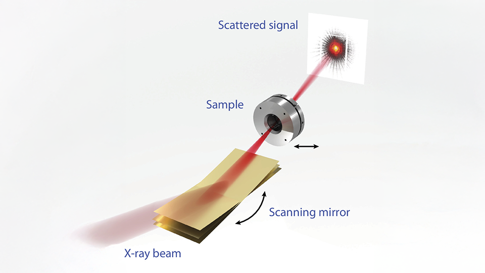
Sometimes a change of perspective can make a world of difference. A team of scientists from PETRA III, Centre for X-ray and Nanoscience (CXNS) at DESY, and MAX IV has rearranged the method in which one can use an X-ray beam to image a sample without using high-quality lenses. The method, called ptychography, has been widely used at synchrotrons and free-electron lasers to analyse the inner workings of materials quickly enough while avoiding major damage to the sample by the X-rays. The team h...
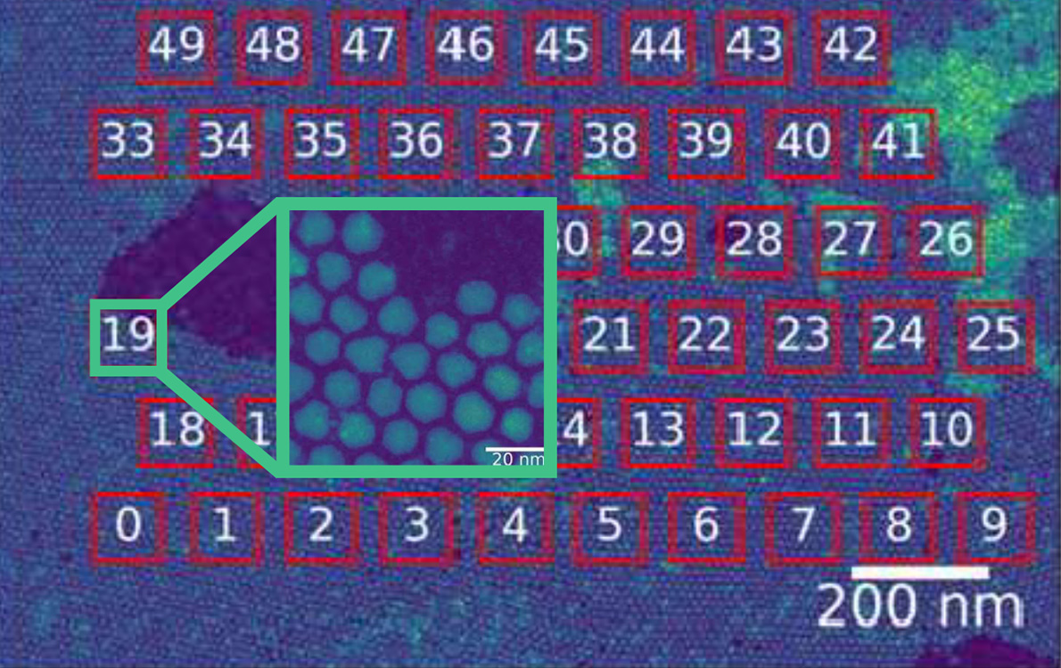
“We now have a way for people to interact with a detector on one side and a supercomputer on the other side with a simple webpage called Distiller in the middle,” said Peter Ercius, interim facility director of the National Center for Electron Microscopy (NCEM) at Berkeley Lab’s Molecular Foundry. “We’re moving towards getting huge amounts of data processed in an automated way with minimal human intervention.”