Helmholtz-Zentrum Dresden-Rossendorf (HZDR)
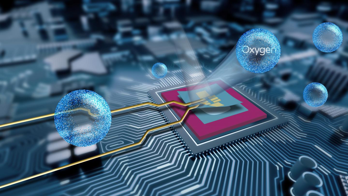
Tomorrow's electronics are getting ever smaller. Researchers are thus searching for tiny components that function reliably in increasingly narrow configurations. Promising elements include the chemical compounds indium selenide (InSe) and gallium selenide (GaSe). In the form of ultra-thin layers, they form two-dimensional (2D) semi-conductors. But, so far, they have hardly been used because they degrade when they get in contact with air during manufacturing. Now, a new technique allows the sensitive material to be integrated in electronic components without losing its desired properties. The method, which has been described in the journal ACS Applied Materials and Interfaces, was developed by Himani Arora, a doctoral candidate of physics at the Helmholtz-Zentrum Dresden-Rossendorf (HZDR).
"We managed to make encapsulated transistors based on indium selenide and gallium selenide," reports Dr. Artur Erbe, head of the "Transport in Nanostructures" group at HZDR's Institute of Ion Beam Physics and Materials Research. "The encapsulation technique protects the sensitive layers from external impacts and preserves its performance." For encapsulation, the scientists use hexagonal boron nitride (hBN). It is ideal for the purpose because it can be formed into a thin layer and is also inert, so it does not respond to its environment.
Indium and gallium selenide are seen as promising candidates for various applications in areas such as high-frequency electronics, optoelectronics and sensor technology. These materials can be made into flake-like films only 5 to 10 atomic layers thick which can be used to produce electronic components of extremely small dimensions.
During encapsulation, the 2D flakes are arranged between two layers of hexagonal boron nitride and thus completely enclosed. The upper hBN layer is responsible for outward insulation, the lower one for maintaining distance to the substrate. The technique was originally developed by the group of James Hone at Columbia University in New York where Himani Arora learned it during a research visit. The doctoral student subsequently continued to work on the topic at HZDR's International Helmholtz Research School (IHRS) NanoNet.
Applying contacts without lithography
One of the particularly big challenges posed by the encapsulation technique was to apply external contacts to the semi-conductors. The usual method of evaporation deposition using a photomask is unsuitable because during this process the sensitive materials come into contact both with chemicals and with air and thus degrade. So, the HZDR researchers employed a lithography-free contacting technique involving metal electrodes made of palladium and gold embedded in hBN foil. This means the encapsulation and the electric contact with the 2D layer underneath can be achieved concurrently.
"In order to produce the contacts, the desired electrode pattern is etched onto the hBN layer so that the holes created can be filled with palladium and gold by means of electron beam evaporation," Himani Arora explains. "Then you laminate the hBN foil with the electrodes onto the 2D flake." When there are several contacts on an hBN wafer, contact with several circuits can be made and measured. For later application, the components will be stacked in layers.
As the experiments have shown, complete encapsulation with hexagonal boron nitride protects the 2D layers from decomposition and degradation and ensures long-term quality and stability. The encapsulation technique developed at HZDR is robust and easy to apply to other complex 2D materials. This opens up new paths for fundamental studies as well as for integrating these materials into technological applications. The new two-dimensional semi-conductors are cheap to produce and can be used for various applications such as detectors that measure light wavelengths. Another example of use would be as couplers between light and electronic current by generating light or switching transistors using light.
Effective hexagonal boron nitride passivation of few-layered InSe and GaSe to enhance their electronic and optical properties
H. Arora, Y. Jung, T. Venanzi, K. Watanabe, T. Taniguchi, R. Hübner, H. Schneider, M. Helm, J. C. Hone, A. Erbe
ACS Applied Materials & Interfaces, 2019
DOI: 10.1021/acsami.9b13442
Contact information:
Artur Erbe | Himani Arora
a.erbe@hzdr.de | h.arora@hzdr.de
Institute of Ion Beam Physics and Materials Research
Phone: +49 351 260-2366

Waste polyamide-derived CQDs show continuous photoluminescence tuning from 308 to 552 nm through sequential defect-state engineering, with optical transition energies decreasing from 4.32 to 2.50 eV. @Christian Ebere Enyoh from Saitama University Carbon quantum dots (CQDs) are fluorescent carbon nanomaterials with potential applications in sensing, optoelectronics, displays, anti-counterfeiting, and environmental technologies. Their optical properties can be adjusted by modifying the carbon...

The researchers used circularly polarized light at normal incidence and found that helicity-dependent photocurrents appeared perpendicular to the crystal’s polarization but vanished when measured parallel to it, supporting a bulk origin of CPGE. @Institute of Science Tokyo The circular photogalvanic effect (CPGE), a phenomenon that generates helicity-dependent photocurrents in noncentrosymmetric materials, can originate purely from a crystal's internal structure without contribution from the...

Summary of gold nanoparticle growth programming in liposome based on localization of biomineralization peptide The position of biomineralization peptides within liposomes can influence how gold nanoparticles grow, reports a research team from Institute of Science Tokyo. Peptides localized at the membrane interface promote branched structures, while those confined to the liposome interior favor spherical nanoparticles. The findings offer a new strategy for controlling nanoscale reaction...
