Friedrich-Schiller-Universitaet Jena
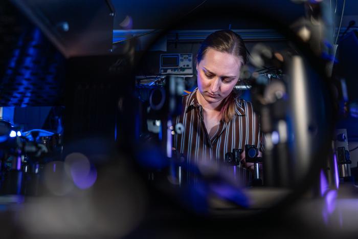
Electrons in a crystal do not simply move like tiny particles along fixed paths. Their behaviour is determined by quantum mechanical states. Researchers summarise the geometric properties of these states under the term »quantum geometry«. An important parameter here is the Berry curvature. Among other things, it influences how electrons react to light or electric fields.
Until now, Berry curvature has mainly been calculated theoretically or investigated using comparatively complex experimental methods. The team from Jena and Regensburg is taking a different approach: it combines optical measurements with an analytical model and is thus able to quantitatively estimate the local Berry curvature of the material.
»We wanted to make a quantum property accessible that has so far been difficult to determine experimentally«, says lead author Nele Tornow from the Institute of Solid State Physics at the University of Jena. »What makes our approach special is that we combine an optical experiment with a theoretical model to obtain a specific value for the Berry curvature.«
Two laser pulses provide the measurement signal
For the experiment, the researchers used tungsten diselenide, a semiconductor whose layer under investigation is less than one nanometre thick. Such atomically thin materials react particularly strongly to light and are therefore well suited to non-linear optical experiments.
The team directed two ultrashort laser pulses at the sample. The first pulse alters the electronic states of the material for a tiny fraction of a second. The second serves to optically detect this change. This produces light at twice the frequency of the incident light. From its polarisation—put simply, the way the light oscillates—the researchers obtain information about the Berry curvature.
The effect takes place within a few hundred femtoseconds. A femtosecond is one millionth of a billionth of a second. If the team changes the direction of rotation of the first, circularly polarised laser pulse, the sign of the measured signal also reverses. From the measurement data, the researchers determined the Berry curvature, which was consistent with theoretical calculations.
»Using this optical method, we can investigate such properties on extremely short time scales«, says Giancarlo Soavi from the Institute of Solid State Physics and the Abbe Centre of Photonics at the University of Jena. »This will enable us in future to track how the quantum geometry of a material changes during very rapid processes.«
Also applicable to other materials
Although the experiment was demonstrated using tungsten diselenide, the research team states that the fundamental approach is not limited to this class of materials. Both the measurement principle and the model—developed in collaboration with researchers from the University of Regensburg—can, in principle, be applied to other materials. In the long term, the method could help to investigate the geometric properties of electronic states in greater detail and to better understand their behaviour in fast optical processes.
Reference
Nonlinear Circular Dichroism Reveals the Local Berry Curvature
Nele Tornow, Paul Herrmann, Clemens Schneider, Ferdinand Evers, Jan Wilhelm, and Giancarlo Soavi
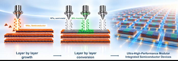
Researchers at the Institute for Basic Science converted a single tungsten diselenide crystal into a working transistor by selectively oxidizing and reacting its top atomic layers. The resulting tungsten oxide served as a sub-nanometer gate dielectric, while tungsten ditelluride contacts cut the charge injection barrier to about a third of that seen with platinum.
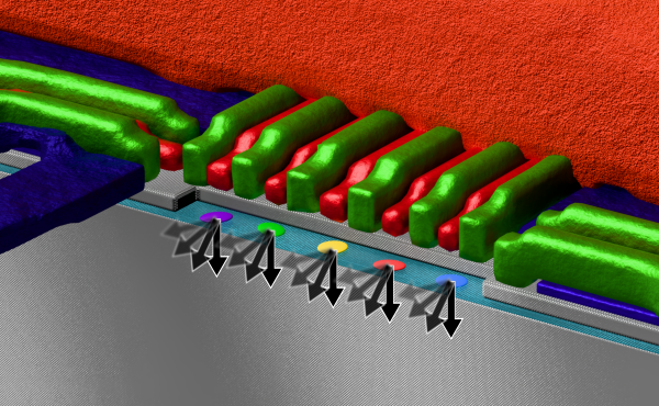
Silicon spin qubits usually lose accuracy when many qubits are driven in parallel, a barrier to scalable quantum processors. Writing in Nature Physics, RIKEN researchers traced the main error source to AC Stark shifts from shared microwave control signals. Their pairwise phase calibration protocol restored gate fidelities above 99.99% for up to three simultaneous qubits, and about 99.9% across all five, near fault-tolerant requirements.
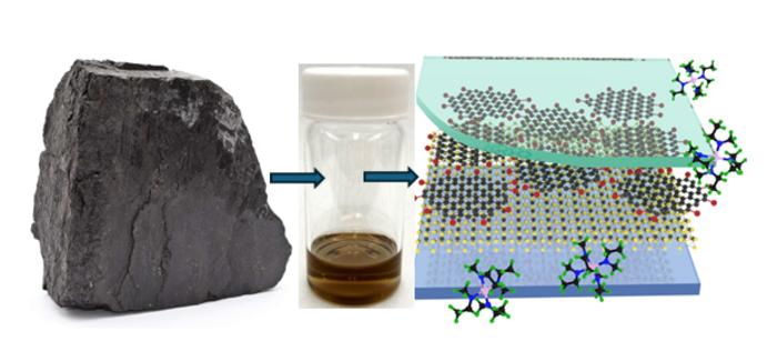
Researchers at the University of Illinois Urbana-Champaign and NETL have shown that carbon nanodots derived from bituminous coal can serve as an atomic-scale interfacial binder for integrating high-κ dielectrics with 2D semiconductors such as molybdenum disulfide.