By Soitec
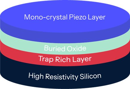
Connect Piezoelectric Materials on Insulators Fusing its elastic wave components expertise with its Smart Cut™ technology, Soitec has developed MultiLayer piezoelectric substrates addressing the demanding RF filters market based on Surface Acoustic Wave technology. The Connect POI substrate, Piezoelectric On Insulators substrate, combined with InterDigital Transducers, enables the creation of high-performance SAW filters that meet the demands of stringent telecommunication bands by offering improved RF performance through a higher quality factor (Q) and lower insertion losses (IL). Additionally, it provides better thermal properties, including a low temperature coefficient of frequency (TCF) and enhanced thermal dissipation. The substrate also supports flexible bandwidth thanks to an appropriate acoustic coupling factor (k²), well-matched phase velocity, and multiplexing capability. Furthermore, it is well-suited for high-volume manufacturing: it offers robustness and compatibility with advanced package and assembly flows for Front-End modules. The multilayers Connect POI substrate is composed of four layers. Used piezoelectric materials are Lithium Tantalate LiTaO 3 and Lithium Niobate LiNbO 3. Connect POI boosts the communications speed & rate between connected equipments, reducing the consumption The versatile Connect POI substrate offers the options to tailor the type of filter skirt of any 5G New Radio band, for any data rate and speed. Coexistence in a massive connected network is not an issue anymore. Nor the integration into compact systems. Connect POI even enables multiplexing to filter several bands on the same die. It also empowers the communication system to lower consumption for data transmission, serving ideally the 5G smartphone and tablet battery life. Connect POI technology makes the bluetooth integration into smartglasses possible: it enables coexistence with the increased allocation of 5G bands thanks to high-selectivity filters! Moreover, the ML-SAW filter on POI is very compact. Moreover, the ML-SAW on POI enables the whole telecommunication channel to work with a lower consumption: perfect for those bright glasses to stay light and longer, with the objective of achieving one operating day without charge-in! Whatever the accuracy requested, for autonomous car or smartphone positioning, the filter needs to segregate the Global Navigation Satellite System (GPS, Glonass, Galileo, BeiDou, NavIC, QZSS) tracking signal from any other transmitted telecommunication. Selectivity, isolation, and low consumption are the Connect POI features enabling this! Achievable miniaturization is an additional benefit for the wearable market! Highlights Gain for Tx filters SAW-ladder— and impedance element filters —, built from series and parallel resonators, take full advantage of POI substrates, where maximized Q factors and ideal coupling deliver steep filter skirts and ultra- low insertion loss. These architectures are well suited to handle maximum incident power. With the Connect POI product, thermal compensation comes from the substrate, there’s no need for an additional deposited layer. Moreover the whole POI structure fosters heat dissipation, responding to the Power Class 1.5 requirements. And no issue with the 50 ohms matching. Gain for Rx filters Connect POI empowers DMS, Double Mode SAW, and innovative architectures, as it offers extremely low Insertion Loss and out-of-band attenuation options. Demanding specifications of Rx filters can be reached, responding to Adjacent Channel Rejection and Adjacent Channel Selectivity requirements. Advantages listed for the Tx filters are also applicable for the Rx filters Multiplexing, from duplexer to x-plexer Duplexer can be designed by combining the both previous approaches of Rx and Tx filters on POI. The Connect POI versatility enables also to integrate, on a same die, some filters addressing different frequencies: diplexer and multiplexer can be then integrated on a single chip, with a single IDT metal layer. Reached cross-isolation or isolation across bands is sufficient between the aggregate paths. Ease of filter manufacturing and assembly The compatibility with multiple IDT technology variants, and advanced package technologies, makes the Connect POI MultiLayer RF Filter easy to produce and integrate. Just a few litho-masks are needed for this process. The Si handle robustness enables the application of advanced packaging technologies, such as fine WLCSP, flip-chip, followed by module assembly, and System in Packages for RFFE modules. One advantage stands in the achievable yields, much better than with TC-SAW technology, particularly for multi-frequency devices. Advantages of a SAW on POI compared to a SAW on piezoBulk The POI multilayers stack offers better waveguide performances, boosting the piezoelectric properties, and limiting its thermoelastic variations. All, on a robust mechanical substrate! Moreover a substrate stack can be designed to optimize performance across various frequency bands, enabling efficient multiplexing! 5G bands selectivity & coexistence with WiFi Connect POI is capable of addressing the whole spectrum, including LTE, 5G, and beyond, enabling energy efficient RF filter designs with compact footprint. Which leads to address multiple markets: Mobile Market, IoT Market, Non Terrestrial Network and SATCOM. Multiple RF filters technologies are available on the market. Connect POI brings up advantages making the MultiLayer SAW filter a major solution of the RF filter market, up to 3+ GHz. Connect POI product portfolio is leveraging Soitec unique Smart Cut™ technology and RF semiconductor expertise.
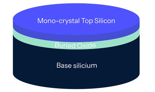
Soitec's Power-SOI empowers electric and autonomous vehicle innovation. Our industry-leading engineered substrates enable the development of advanced automotive applications, delivering superior energy efficiency, performance, robustness, integration, sustainability, faster time-to-market and intelligence. It meets enhanced FuSa standards and 48V architecture requirements. Power-SOI Features & Benefits High voltage & low voltage integration on the same die: Power-SOI with DTI (deep trench isolation) enables integration of high and low voltage blocks on a single die, minimizing die area. High temperature operation: Power-SOI's superior low leakage at high temperatures enhances temperature margins, facilitates AEC-Q100C Grade 0 certification, and improves device accuracy. High robustness: Power-SOI's excellent noise immunity, latch-up-free structure, and enhanced ESD/EMI/EMC properties enable high-performance power ICs that meet stringent robustness requirements. Simple device design: Power-SOI simplifies device design, reducing mask count and eliminating complex well structures. It also improves BV-Rsp performance through double RESURF High Efficiency: Power-SOI technology often enables devices to work with higher efficiency by offering the lower on resistance (RDSon) and lower reverse recovery charge (Qrr). This benefit is crucial for energy-sensitive applications, particularly in automotive and mobile devices, contributing to longer battery life and energy-efficient performance. Scalability for Future Nodes: Power-SOI is highly scalable for future technology nodes, making it adaptable to evolving needs in semiconductor manufacturing. This scalability ensures that Power-SOI will remain relevant in future generations of ICs, allowing for integration of new functionalities without increasing die size or complexity. Connecting the world with Soitec Power-SOI substrates Soitec's Power-SOI substrates enable smart power management in electric vehicles (EVs) and advanced driver-assistance systems (ADAS), meeting high functional safety standards and supporting 48V low-voltage architectures for better efficiency. Their robustness and high-temperature tolerance make them ideal for powertrain and under-hood components. In industrial applications, Power-SOI substrates offer durability, noise immunity, and energy efficiency, simplifying power IC design by integrating high- and low-voltage components. They are essential for reliable operation in harsh environments, particularly in motor drives, inverters, and automation systems. Power-SOI substrates enhance energy efficiency and performance in datacenters and network infrastructure by supporting efficient power supply circuits and high-speed signal processing. Their ability to operate in high-temperature environments ensures reliable performance in demanding computing and telecommunication systems. Highlights Efficient smart power IC: Power-SOI improves 10% system cost and smart power IC efficiency. Safer smart power IC: Power-SOI facilitates smart power IC development, meeting high robustness, noise immunity, and operating temperature requirements. Better performance smart power IC: Power-SOI improves 10% system cost and smart power IC efficiency. Increased Voltage Handling Capacity: Power-SOI enables high voltage isolation capabilities, supporting up to 200V in smart power ICs. This allows for better integration of high-voltage and low-voltage components on the same die, which is essential in applications like power converters and motor drivers. Frequently asked questions Which applications use Power-SOI? - IVN (In-vehicle Networking) such as CAN, LIN, FlexiRay, Ethernet Phy ICs - PMIC (Power Management IC)/ SBC (System Basis Chip) - BMIC (Battery monitoring IC)/ BMS AFE (Battery management system analog front end) - Gate driver IC - Smart actuator/ smart motor controller IC - Industrial interface IC - HiRel (High Reliability) IC etc. What are the benefits of using Power-SOI? - To enable high integration of high voltage circuits and low voltage circuits on the same die for saving die area - To provide high robustness and reliability for meeting higher functional safety (FuSa) requirements - To ease the IC design with increasing demands of wider operating temperature and higher FuSa requirements - To shorten the IC development time by ensuring higher percentage of first time right design which improves the time-to-market - To improve the efficiency of the power IC by reducing the conduction losses and switching losses What are the key inflections that Power-SOI addresses? - The new 48V low voltage architecture: Power-SOI enables higher breakdown voltage (BV) which is needed for this architecture (said 200V BV) - Increasing demands for higher functional safety (FuSa): Power-SOI enables the integration of high voltage circuits and low voltage circuits by providing excellent noise immunity with DTI & BOX, latch-up free structure and significant reduction of isolation area - Package downsizing: Power-SOI low leakage current at higher junction temperature and much smaller die size allow the use of smaller package size How many product families are inside Power-SOI product portfolio? 200mm Power SOI - Smart Power 1.5: SmartCut ™ SOI EPI ready only up to 1.5um SOI thickness with BOX up to 3.0um - Smart Power 2.0: SmartCut ™ SOI + EPI (up to 10 um) with BOX up to 3.0um - Smart Power 2.1: SmartCut ™ SOI + EPI (up to 10um) with 3.1um to 3.9um BOX 300mm Power SOI - Smart Power 3.0: SmartCut ™ SOI EPI ready only up to 0.2um SOI thickness with BOX up to 2um - Smart Power 3.1: SmartCut ™ SOI + EPI (up to 7um) with BOX up to 2um
CATEGORY
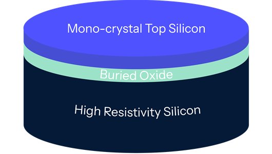
Photonics-SOI from Soitec is an advanced technology platform that integrates photonic components on a silicon-on-insulator (SOI) substrate to enhance optical communication capabilities. Photonics-SOI offers significant advantages for optical transceivers, including high data rates, cost efficiency, power savings, compact size, and improved signal integrity. These benefits make it a compelling choice for high-speed data center interconnect applications. Photonics-SOI provides several advantages for personal healthcare sensors, including miniaturization, cost efficiency, high sensitivity, and integration capabilities. These benefits enable the development of advanced, compact, and accurate monitoring devices for health applications. Photonics-SOI is used in Light Detection and Ranging (LiDAR) devices which are increasingly being used in Advanced driver-assistance system (ADAS), mobile and consumer applications. Photonics-SOI enables the implementation of Quantum Key Distribution (QKD), a method for secure communication based on quantum principles. Silicon-based photon sources and detectors can be used to create and distribute quantum keys between parties, ensuring secure data transmission. Enhanced Bandwidth and Speed The technology supports high-bandwidth and high-speed optical communication, addressing the increasing demands for data transfer in data centers, telecommunications, and computing systems. Integration and scalability By leveraging silicon’s established manufacturing processes, Photonics-SOI supports scalable production and seamless integration with existing silicon electronics, facilitating the development of compact, high-density optical systems. Reduced power consumption Photonics-SOI contributes to lower power consumption by utilizing optical signals for data transmission, which is more energy-efficient than traditional electrical interconnects, especially over long distances. Soitec provides innovative solutions for high speed and robust connectivity in data center interconnect and network infrastructure connectivity. By offering superior thermal management and reduced power consumption, Soitec's substrates help optimize the operation of servers and networking devices, enabling faster data processing and lower energy usage. Soitec offers a portfolio of solutions which enhance the performance and efficiency of Edge AI and IoT applications. By providing high-quality, energy-efficient substrates, Soitec helps to optimize IoT devices by enhancing their reliability and extending battery life, making them ideal for real-time data processing and communication in various applications. Soitec empowers electric and autonomous vehicle innovation. Our industry-leading engineered substrates enable the development of advanced automotive applications, delivering superior energy efficiency, performance, robustness, integration, sustainability, faster time-to-market and intelligence. Soitec empowers smart industrial applications and enables industry leading industrial automation. Our industry-leading engineered substrates enable the development of advanced industrial applications, delivering superior energy efficiency, performance, robustness, integration, sustainability, faster time-to-market and intelligence. Current world’s semiconductor capacity and the demonstrated large scale manufacturability of engineered substrates have provided the possibility for every person in the world to afford at least one device - a smartphone for most - able to acquire, process and communicate information of its surroundings. As the leader in engineered substrates, Soitec is helping enterprising customers and partners in ensuring that their products meet the ever-increasing expectations in consumers' Quality-of-Experience. Our engineered substrates help ensure end-to-end energy efficiency, fast, secure and reliable data acquisition and processing and robust broadband connectivity. In what applications is Photonics-SOI being used? Photonics-SOI is used in a wide range of applications from data center interconnect, LiDAR, personal healthcare to quantum technologies. What are the benefits of using Photonics-SOI in an optical transceiver? Photonics-SOI offers the advantages of enhanced bandwidth and speed, higher integration and scalability, and reduced power consumption.
CATEGORY
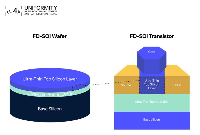
FD-SOI enables energy efficiency and seamless connectivity FD-SOI technology provides the optimal balance between digital performance, mixed signal/RF compatibility, power consumption and cost. The ultra-thin film FD-SOI architecture enables transistors to operate in fully depleted mode, offering an “electrical Shrink-on-Chip” solution while simplifying the manufacturing process. How FD-SOI will impact your products Low Active Power Consumption FD-SOI outperforms alternative technologies in terms of energy efficiency at a given technology node. Performance on demand Body bias feature provides a very powerful knob for fabrication process, voltage, temperature and aging (PVTA) compensation and performance boosting. Ultra-low leakage with ultra-low VDD - Always ON FD-SOI is an ultra low-voltage technology which is able to operate at very low VDD at minimum energy per operation. Compact Solution FD-SOI enables easy digital / analog RF integration which offers an optimum solution for wireless connectivity applications. Superior RF Performance Planar FD-SOI technology reduces parasitics, enabling higher ft/fmax values - key for pushing the limits of RF design performance. Enhanced Noise Immunity for RF Applications Thanks to their insulating layer, FD-SOI substrates offer superior interference isolation, making them ideal for highly integrated RF and analog mixed signal circuitry in 5G mmWave, Wi-Fi, Bluetooth and a wide range of other wireless systems. Where FD-SOI technology is being used Soitec offers a portfolio of solutions which enhance the performance and efficiency of Edge AI and IoT applications. By providing high-quality, energy-efficient substrates, Soitec helps to optimize IoT devices by enhancing their reliability and extending battery life, making them ideal for real-time data processing and communication in various applications. Soitec provides innovative solutions for high speed and robust connectivity in data center interconnect and network infrastructure connectivity. By offering superior thermal management and reduced power consumption, Soitec's substrates help optimize the operation of servers and networking devices, enabling faster data processing and lower energy usage. Soitec empowers electric and autonomous vehicle innovation. Our industry-leading engineered substrates enable the development of advanced automotive applications, delivering superior energy efficiency, performance, robustness, integration, sustainability, faster time-to-market and intelligence. Soitec empowers smart industrial applications and enables industry leading industrial automation. Our industry-leading engineered substrates enable the development of advanced industrial applications, delivering superior energy efficiency, performance, robustness, integration, sustainability, faster time-to-market and intelligence. From MHz to mmWave frequencies, semiconductors built on Soitec’s FD-SOI substrates consistently deliver high performance and low power consumption across a wide range of wireless applications - from IoT and smartphones to 5G mmWave and advanced terrestrial and satellite networks. Highlights Widely used in major smart watches and hearing aids. Widely adopted in leading 5G mmWave-enabled smartphones. Widely adopted for next-generation radar SoCs for the automotive industry. Widely used in advanced driver assistance systems (ADAS), FD-SOI technology helps ensure reliability in harsh environments while maintaining energy efficiency. FD-SOI substrates form the basis for energy-efficient AI processing. Frequently asked questions In what applications is FD-SOI being used? Due to its unique superior characteristics, FD-SOI is used in a wide range of devices from a low power microcontroller, embedded wireless controller, radar and mmWave. These devices are used in market segments from wearable and hearable, automotive infotainment system, software-defined vehicle, mobile and consumer. What are the benefits of FD-SOI? FD-SOI technology allows always-on feature and longer battery life-time in a battery-operated smart home or wearable device. It provides digital and analog/RF integration which makes it an ideal solution for wireless controllers used in IoT, mobile and automotive radar applications.
CATEGORY

Advanced substrates offer higher precision, enhanced mechanical performance, and lower power consumption for high-performance sensors MEMS-SOI enhances sensor performance Soitec's MEMS-SOI offers the benefits of higher precision, enhanced mechanical performance and lower power over traditional MEMS technologies to high performance sensors. MEMS-SOI sensors benefit from improved sensitivity due to reduced electrical and mechanical noise, allowing sensors to detect smaller changes in the measured parameter more effectively. The reduction in parasitic capacitances and the improved isolation provided by the SOI substrate can lead to faster response times for MEMS sensors. This means that sensors can react more quickly to changes in the measured parameter, which is crucial for dynamic applications. How MEMS-SOI will impact your products Higher precision and accuracy SOI substrates offer a high degree of uniformity and precision in device fabrication, leading to more consistent and reliable MEMS devices. This is particularly important in applications requiring tight tolerances and high performance. Enhanced mechanical performance The SOI substrate provides a high-quality, low-stress silicon layer that improves the mechanical properties of MEMS devices. This can lead to better precision, higher resonant frequencies, and improved stability of MEMS structures. Reduced power consumption MEMS-SOI devices typically exhibit lower power consumption compared to traditional MEMS technologies. The reduced parasitic capacitance and efficient thermal management contribute to lower energy requirements, which is beneficial for battery-operated and portable applications. Where MEMS-SOI technology is being used Edge AI & Internet of Things MEMS-SOI enhances the user experience in AR/VR glasses and headsets by enabling chipsets to do real-time motion detection, precise head tracking, and eliminating image distortions for a more immersive experience. Automotive MEMS-SOI enables accelerometers and gyroscopes that are used in airbag systems to detect rapid deceleration and activate airbags instantly during a collision. They also support stability control, traction control, and anti-lock braking systems (ABS) by monitoring vehicle dynamics. Mobile & Consumer MEMS-SOI enables sensing solutions that are present in devices we use everyday, such as smartphones, hearable and wearable, where they enable a variety of tasks such as image stabilization, user interfaces and power management. Industrial MEMS-SOI enables accelerometers and vibration sensors to monitor equipment health by detecting early signs of wear, misalignment, or malfunction. This data enables predictive maintenance, reducing downtime and repair costs by addressing issues before they become critical. Frequently asked questions In what applications is MEMS-SOI being used? MEMS-SOI is commonly used in high performance sensors. These sensors can be found in a wide range of applications from Edge AI and IoT, Industrial, Automotive, Mobile and Consumer market segments. What are the benefits of MEMS-SOI? MEMS-SOI provides the essential features to a high performance sensors in terms of higher accuracy, shorter response time, increased mechanical ruggedness and lower power consumption.
CATEGORY
