By Global TCAD Solutions (GTS)
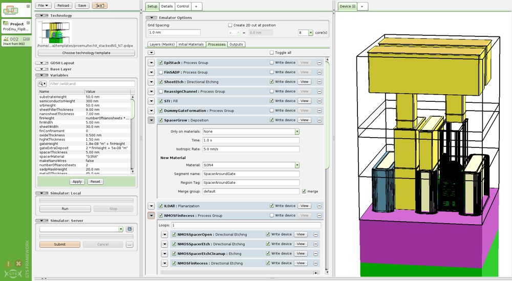
A Rich and Powerful Process Emulator GTS ProEmu conveniently brings the process to DTCO – a perfect match with GTS CellDesigner: Understand how each process step affects subsequent steps as well as device performance. Combine process modules to quickly explore new process flow designs and assess variability and yield. Tune your technology, leap ahead. Applications ProEmu integration with Cell Designer: GDSII masks, process modules and steps, device generation, parasitics extraction (PEX) - Process flow design - Variability & yield - DTCO Explore Key Technology Parameters with Design and Process in Mind - Variability in masks & processes - Identify critical process steps - Examine effects down the line - Study the impact on reliability Technologies differ increasingly. Optimize your process to get the most out of your FinFET, NSFET, NWFET, and CFET designs. Emulation Models / Process Steps Nanosheet process flow created with ProEmu Emulation - Etching - Deposition (CVD) - Spin-On-Glass (SOG) - Selective Epitaxial Growth (SEG) - Wet Etching Geometric Models - Planarization (CMP) - Fill - Directional Etching - Geometric Ion Etch Material Operations - Add Material from Shape - Cut-out Material with Shape - Subtract (present or inverted) Shape from Material - Remove Material - Move Material Vertically Analytical Doping Operations - Add Doping from Mask - Add Doping from Equation - Remove Doping Process Modules and Output - Process Group (Contains a number of processes) - Output for visualization and device simulation For process simulation, see GTS ProSim. Integration with Process-Aware DTCO Process-aware DTCO flow with GTS CellDesigner and ProEmu Use your mask layouts and customize easy-to-use technology process flows to investigate single devices, cells, and circuits. Add process variation in your flow and understand critical process steps and their impact on power, performance, variability, and reliability. Use predictive device simulations (NDS), TCAD calculations, and SPICE in Unison to optimize your process, design, and technology. Open to Integration with Other Tools Besides being embedded in GTS Framework for easy setup of workflows (e.g., with GTS CellDesigner), including the DoE (splits) tool and integrated optimizer, ProEmu can easily be used in combination with other tools. - Integration with process simulation - Wide interoperability with 3rd-party tools Environment - Integration in GTS Framework (DoE, Optimizer, workflows, device, and circuit simulators) - Intuitive and versatile graphical user interface - Comprehensive scripting interface - Efficient multi-core simulation support A Dependable Companion for Process Emulation in all Contexts - Flexibly change and combine process modules - Investigate the impact of each process step - Full interoperability with process simulation - Reliability & variability comprehensively covered - Robust and computationally efficient - Full integration with TCAD and DTCO
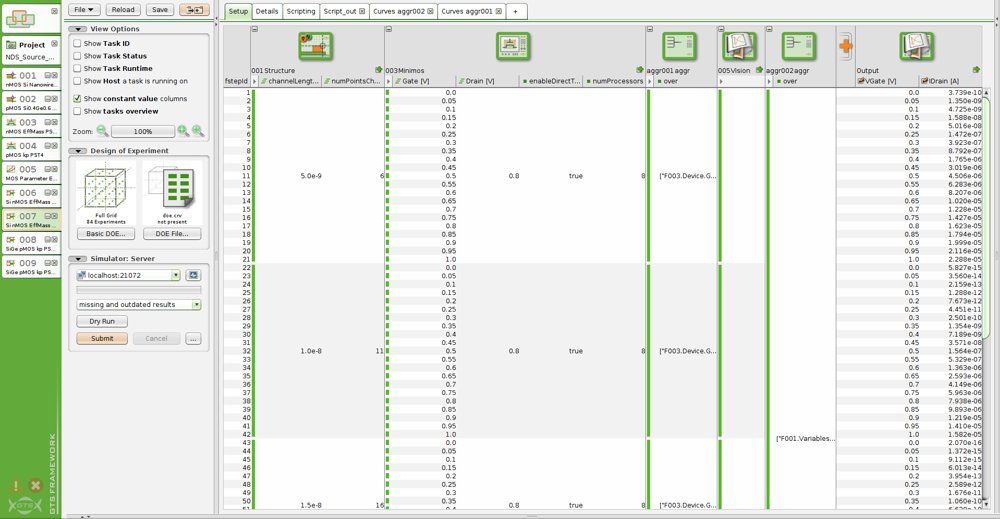
GTS Framework is our base work environment for TCAD applications. Designed as a framework, it embeds various programs (“tools”) in a common workspace, and provides workflow and automation functions like splits/DOE-setups and automatic optimization, backed by structured file storage. All these features are provided in an intuitive (graphical) user interface that is consistent for all tools. Thus, GTS Framework offers unprecedented ease-of-use, allowing even first-time users to get productive within a few hours – proving GTS Framework an extremely efficient working environment. In demanding R&D tasks as well as in production work with tight timelines, being able to focus on the actual simulations and on examining the results is key to efficiency and fast progress. GTS Framework contains all necessary elements, being a solid base for your workflow. It includes essentials such as file I/O, structured data storage, and network integration – up to higher-level functionalities such as setup of experiments and workflows (including splits/DOE and optimization) and automated task distribution in computational clusters. GTS Framework is known for its industry-leading user interface, which helps the beginner yet satisfies the expert – allowing users to choose their preferred way of working. This holds for the 3-level simulator configuration (see below), but e.g. also for its transparent file storage. With the included Tutorials and Application Examples, users get productive even more rapidly. GTS Framework includes an Optimizer as well as features for running experiments with splits or more complex DOE (design of experiment) setups. The respective tasks run locally or on a cluster, automatically distributed via GTS JobServer. Features: - Creation, importing and editing of 1D/2D/3D device geometries - Classical device and circuit simulation, mixed mode - Quantum-mechanical device simulation - Instant 1D/2D/3D visualization of results - Easy-to-use, consistent graphical user interface for all tools (SmartConfig) - Tutorials and examples for quickly achieving results - Scripting tool for complex workflows and data processing (GTS Script, Python) - Powerful and extensible Input Deck Programming language (IPD) - Structured but straight-forward file management for efficent workflow (projects, ToolFolders, NextTool widget) - Remote queuing and execution of simulation jobs / distributed computing (GTS Net+Script+JobServer) - Remote project storage / sharing data in workgroups (GTS Net+JobServer) - Support for multiple platforms (Linux, Windows) - Support for clusters (SGE, LSF, plain TCP/IP) GTS Framework is the preferred environment for using GTS TCAD tools, and it can integrate third-party tools as well. As a comprehensive and flexible platform, GTS Framework helps concentrating on your simulations and results: Implementing workflows is easy and efficient, due to a consistent hierarchical user interface, transparent file management, and distributed computation. The built-in Optimizer and DOE functions provide easy automation of complex experiments. Integration and interoperability with third-party tools make GTS Framework a valuable platform to rely and build upon, both from an operational as well as from a strategic view.
CATEGORY
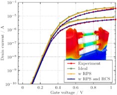
Profound Physical Device Simulation GTS Nano-Device Simulator (NDS) is the first fully integrated solution for effective physical simulation of nano-scale MOSFETs independent of their technology nodes. NDS is built around a solver for the subband Boltzmann transport equation and provides complete coverage of short-channel effects, including velocity overshoot and source-drain tunneling. NDS is the tool of choice for profound predictive simulation of current and future CMOS technologies. NDS is an advanced device simulation tool based on the solution of the subband Boltzmann transport equation (SBTE) in a critical region of the device such as the channel. NDS incoroprates the electrostatic and near-equilibrium transport from Minimos-NT, and the subband structure calculation and scattering models from VSP. It further extends the SBTE with tunneling transport based on the WKB approximation. As such, NDS can accurately account for material characteristics, crystal orientation, stress, quantum effects, ballistic and kinetic (non-equilibrium) transport effects, all in one package based on solid physical background. The integration with the classical simulator Minimos-NT provides flexibility, stable convergence, and ease-of-use. Despite its sophisticated physical models NDS can be operated just like a classical drift-diffusion-based simulator. In an NDS simulation, a critical region of the device such as the channel is partitioned along the transport direction into slices. After computing an initial solution using Poisson/drift-diffusion, NDS invokes a Schrödinger solver on each slice to account for quantum confinement and to calculate scattering rates. Based on these results, the SBTE is solved in the critical region and SBTE solution converted into an effective mobility that is passed back to the Poisson/drift-diffusion equations. This process is repeated until convergence is reached. NDS can efficiently simulate the whole range of device characteristics using just one simulation setup and run. In this way, the user can obtain both accurate and fast device simulation results for various device architectures, materials and bias points. NDS accounts for all physical phenomena relevant for operation, performance, and reliability of nano devices, such as material characteristics, crystal orientation, stress, ballistic effects, scattering, direct tunneling, band-to-band tunneling, etc. In one single simulator setup, NDS can predict transistor performance parameters like electron mobility, I ON, I OFF, sub-threshold slope, DIBL, leakage, and more — all based on physical simulation relying on material properties rather than empirical models. At the same time, NDS simulations have short turn-around times that make it well-suited for day-to-day use in TCAD. NDS Capabilities Drive Current (I ON) - Boltzmann transport equation - Ballistic and dissipative transport - Velocity overshoot - Quantum resistance - Performance enhancement by channel strain Off-state Leakage (I OFF) - Quantum-mechanical transport - Direct SD-Leakage - Band-to-Band Source-Drain leakage NDS Models NDS leverages the microscopic models available in VSP and combines them with a phase-space transport (PST) solver to solve the SBTE. By using the same band structure and scattering models as VSP, NDS makes it possible to cross-calibrate and transfer model parameters between the two tools - see model building in path-finding for silicon. Band Structure Models are consistent with the ones used in VSP. - Effective mass approximation (EMA) or k·p-based Hamiltonians - Quantum confinement giving rise to subband structure - Arbitrary crystal orientations - Responds to mechanical stress through deformation potentials Scattering Models are consistent with the ones used in VSP. - Acoustic phonon scattering - Optical and inter-valley phonon scattering - Polar-optical phonon scattering - Surface roughness scattering - Coulomb scattering from local and remote sources (dopants, oxide charges and dipoles, traps) - Alloy disorder scattering Phase-Space Transport - Solution of coupled mulit-subband BTE in r–k-space, i.e. phase space for electrons and holes - Electron/hole distribution function of position, momentum, and energy gives detailed insights into device operation at any bias - Semi-classical transport: ballistic transport & scattering - Pauli-exclusion, Fermi-Dirac statistics - Crystal orientation and strain effects automatically included through subband structure - Multi-dimensional: planar and non-planar devices - Adaptive r, k, and energy grids for maximum simulation performance Tunneling Transport - Intra-band source-drain tunneling, Schottky-barrier tunneling, band-to-Band tunneling - Transmission coefficients computed using WKB approximation - Based on numerical computation of complex (sub-)band structure - Seamless integration of tunneling rates within PST - Tunneling included in PST with virtually no added run-time or memory cost - Accuracy verified against ballistic NEGF Environment - Integration in the GTS Framework - Graphical user interface - Sophisticated input-deck database - Multi-core simulation support - Material database extendable via C++ like script language - Import of third-party device geometries and meshes NDS – The Sound Choice for New Challenges True physical simulation is the only way of getting profound data for device shrinking, and for designing, optimizing and predictively evaluating new device architectures and new materials. As a unique, well-maintained, modular and expandable physical modeling platform but one which can deliver accurate results in reasonable time, GTS Nano-Device Simulator is the sound choice for years to come.
CATEGORY
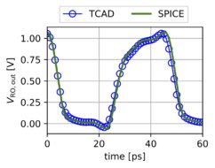
GTS Cell Designer is a tool suite for planning and implementing advanced DTCO workflows – combining layout-based structure generation incorporating detailed technology information (accounting for variability) and advanced physical device and circuit simulation in a parametrized and customizable environment. The Smarter Approach to Design-Technology Co-Optimization Deciding on a technology has big implications from device and cell to circuit and system level. With GTS Cell Designer you can benchmark your technology options (FinFET, NWFET, NSFET, CFET, VFET and more) and get the best design for each. Use the device parameters calculated by GTS Nano Device Simulator (NDS) combined with technology information to obtain an accurate 3D TCAD model of your logic cell. With the automated Spice Model Extractor and the field-solver based parasitics extraction (PEX) you will obtain an accurate circuit representation from a fully consistent TCAD flow. Study cell and device variability, calculate parasitics, power-performance-area (PPA), and gain insight on variability and reliability of the circuits. Optimizations can be run for various aspects – see Cell/Circuit Optimization. - Power, Performance, Area (PPA) - Parasitics - Thermal robustness - Reliability, time-to-failure - Variability, process variations Focus on Your Application Explore key technology parameters which you get from your Cell Designer DTCO workflows. No need for hard-to-obtain process data, no need to dig into process details but focus on achieving your application target Built on Experience, Matured with Industry Feedback Based on its scientific and practical expertise in device simulation, as well as feedback from customers, GTS has prepared example workflows matching the needs of the semiconductor industry. In contrast to conventional, process-related solutions, the required amount of input data for a full-fledged DTCO workflow is moderate and well obtainable – a key aspect when working with contractors. GTS Cell Designer satisfies the demands for reasonable turn-around execution time, and features automatic extraction of key technology parameters as results. With all tools originating from one source, sharing interfaces and data structures, GTS is delivering a consistent solution which is easy-to-use yet powerful and customizable. For Verification – Full TCAD DTCO With the GTS Spice Model Extractor and the GTS Parasitics Extraction as part of the Cell Designer DTCO flow, a completely consistent TCAD-based characterization of the standard cell becomes possible for the first time. Some might say you should never go full TCAD, but with that in mind, the results can be easily verified by running our full TCAD DTCO flow with only four tools in the chain. As shown here, the calculated transients from the TCAD and Spice approach are in excellent agreement giving credit to our fast but accurate Spice DTCO flow. As Cell Designer user you can always verify your results. Modular, yet Compact – a Comprehensive Solution GTS Cell Designer is more than just a combination of individual tools. While each step of the workflow is executed in a separate simulation tool (e.g. Structure, Minimos-NT, VSP) or data processing tool, the workflow (scheduling, distributed execution, post-processing, visualization) is an automated, integrated process in GTS Framework / Cell Designer. Features - Parameterized layout templates as well as a GDSII layout editor - Fast and reliable 3D structure generation, including doping and meshing, fully configurable - Full 3D transient mixed-mode device simulation - Variability, reliability for aging-aware DTCO - Spice Model Extractor: fully automated and scriptable generation of BSIM model cards - Resistance and capacitance extraction of FEOL, MOL and BEOL in one go - Netlist generation - Spice simulation for PPA extraction using internal Python based solution or 3rd Party solver - Data-analysis and post-processing using flexible Python modules GTS Cell Designer alleviates the major issues faced by conventional DTCO approaches. Cell Designer generates realistic but simulation-ready cell geometries without the need for hard-to-obtain process details. You get improved turn-around times and a solid, physically sound base for model calibration. Cell Designer integrates the flow in one familiar user interface, providing automated Spice model and parasitics extraction while still allowing for full customization by DOE/splits, parameters, scripting, etc. Application examples and tutorials ensure a quick start.
CATEGORY
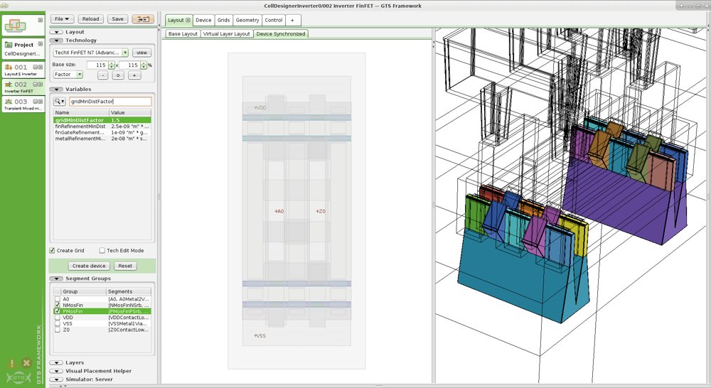
GTS Structure is an intuitive tool for definition and modification of device structures; its state-of-the art graphical user interface facilitates highly efficient use – a significant advantage over conventional solutions. A Powerful Structure Generator and Editor GTS Structure is first-choice for creating simple test devices as well as sophisticated real-world structures. Using the built-in 2D/3D CAD editor, devices can be either designed from scratch, or created/edited based on a comprehensive set of parametrized templates. Alternatively, a module for Layout-based Structure Generation (LSG) capable of reading GDSII mask files can be used to generate device structure from layout using a matching technology rules file. Furthermore, GTS Structure provides an intuitive meshing engine for creation of structured as well as unstructured meshes in two and three dimensions. It offers various manual and automatic mesh refinement options. Device structures can be imported from other TCAD formats / 3rd-party process simulators as well. Structure quantities such as doping and material properties can be defined by analytical functions in the CAD editor, or can be imported from third-party device and geometry files. Features Layout-based Structure Generation (LSG) Inverter cell created from layout (N7 FinFET technology) - Reading mask files - Customizable sets of technology rules - Geometric variability - Generate structures ready for 3D simulation - Multiple structures from same layout Graphical Structure Editing CAD Device Editor - 3D CAD editor for arbitrary device structures - Graphical geometry editor - Graphical doping editor - Extensive library of customizable device templates - Import from 3rd-party process simulators / file formats Graphical Quantity Editing - Quantity editor using analytical expressions - Quantity interpolation from various input files Advanced Meshing 3D unstructured mesh generation - Robust and easy-to-use meshing engine - Unstructured and structured meshes - Quantity-based multiple mesh refinement Environment - Integration in GTS Framework - Intuitive and versatile graphical user interface - Comprehensive scripting interface Versatility and Speed Structure generation and preprocessing is an important prerequisite for accurate and effective device simulation. In order to be useful, a structure generator should provide for simple definition/import and modification of industry-relevant device structures. Generated mesh should reflect relevant structure characteristic and also be suitable for device simulation. GTS Structure provides all those benefits and more. Avoiding the computationally intensive tasks of process simulation or emulation, which additionally require non-disclosed input from a foundry, it uses the fast LSG method to deliver realistic (and large) device structures with meshes optimized for device simulation. For even more realistic structures, structure generation and LSG and can be enhanced with imported geometries, meshes, and attributes.
CATEGORY
