By XRnanotech
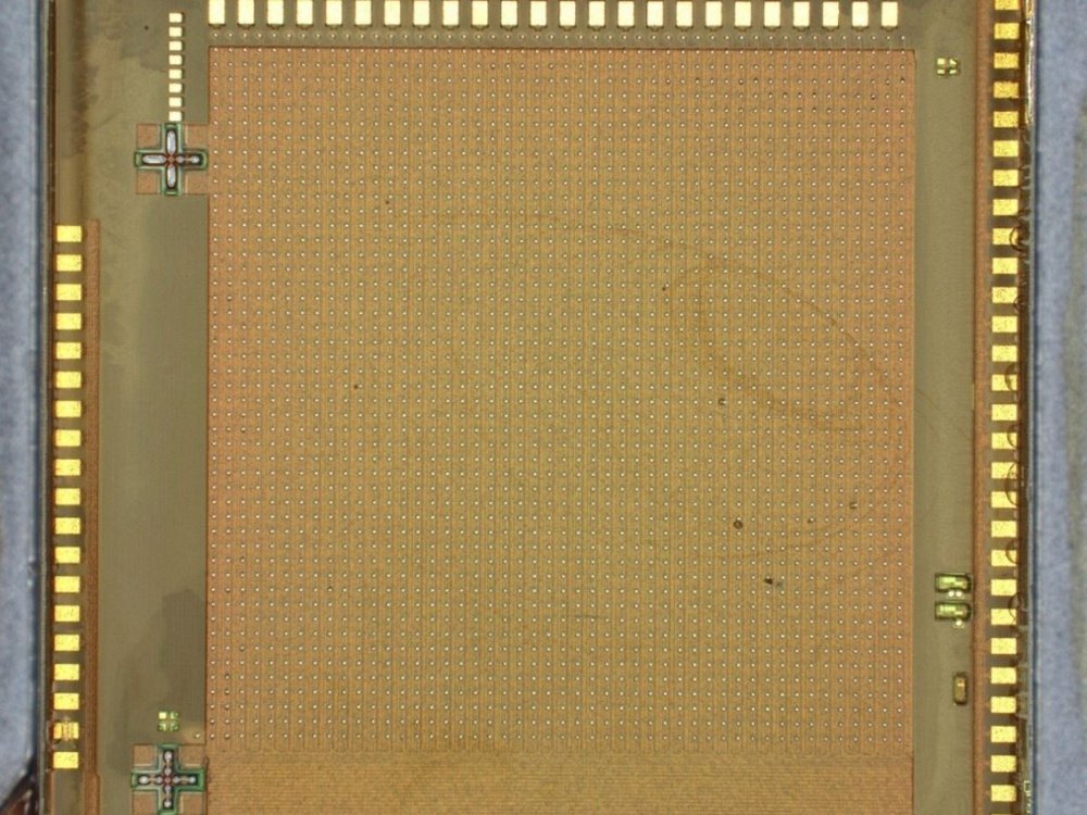
Using lithography, we develop and fabricate detector chips, sensors, and integrated circuits for your specific applications.
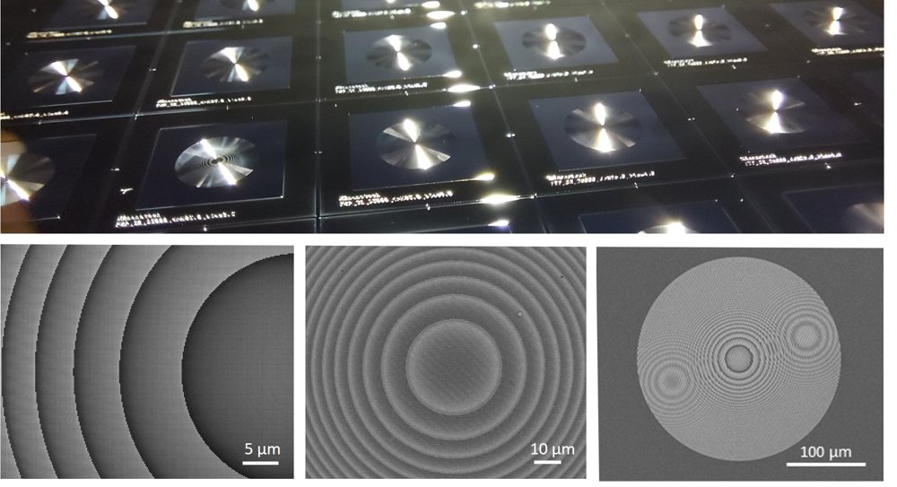
Nanostructured meta- optical components for precise wavefront control and efficient light focusing from VIS to SWIR wavelengths, enabled by XRnanotech’s high-resolution nanofabrication for customized, high-performance and compact optical solutions. - Nanostructured metalenses for advanced wavefront control - Meta-optical components for compact high-efficiency focusing - Compatible with multiple material platforms including SiO₂, TiO₂, and metallic structures - Applicable in medical devices, IR imaging and in VIS applications like machine-vision Metalenses based on nanoscale meta-optics enable precise control of light with compact, highly efficient optical elements, opening new possibilities for advanced imaging, photonics, and quantum technologies. Specifications Large Material Choice SiO 2, TiO 2, HfO 2, SiN, AlN, Polymers, etc. Different Substrate Possibilities Si, SiN, SiO 2, etc. Applications Cameras, AR/VR, Compact Imaging Setups, Quantum Sensing, LiDAR, Integrated Photonics, Space Applications
CATEGORY
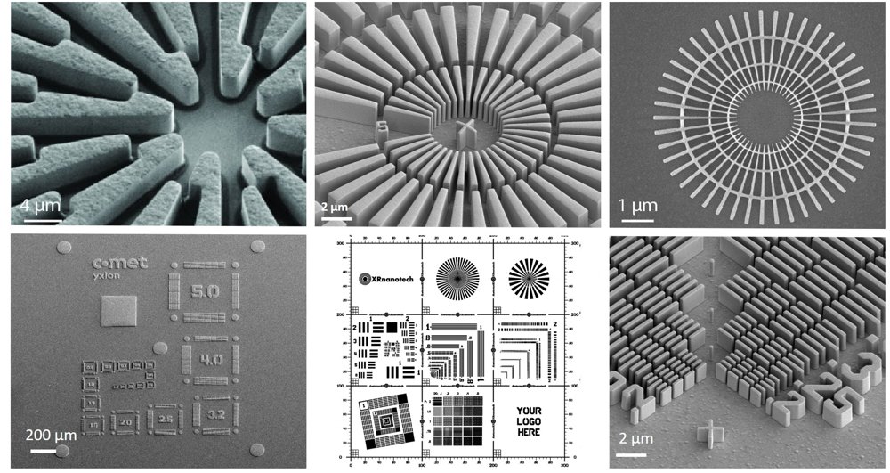
Quality control and machine performance verification devices - Various standard resolution test patterns - High contrast material choice: Au, SiO2 - Customizable according to customers’ needs - NanoXSpot, USAF 1951, Yxlon, Siemens stars We offer a broad portfolio of standard resolution targets, including YXLON, NanoXSpot, and USAF 1951, covering a wide range of precision requirements. Our capabilities extend to fully customized designs – from Siemens stars to nested-L patterns – tailored for advanced imaging and metrology applications. Specifications Smallest Features / nm, Height, Aspect Ratio Ultra-high Resolution: 10 nm, 0.2 µm, 20: 1 High Resolution: 50 nm, 0.8 µm, 16: 1 Microscopy Target: 100 nm, 1 µm, 10: 1 Micro-CT Target: 200 nm, 1.5 µm, 7.5: 1 Calibration Target: 300 nm, 4 µm, 13: 1 Calibration target: 400nm, 4 µm, 10: 1 Prices per piece with volume discounts applicable.
CATEGORY
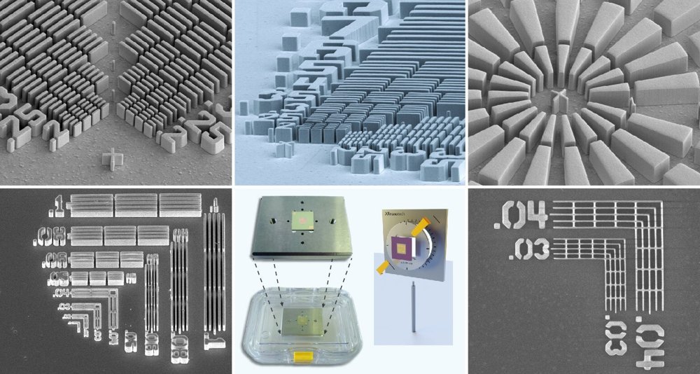
Electron-beam lithography-based fabrication with optimized writing strategy. - Calibration standards - Resolution test targets - Fast Lead time - Material choices: Au, Ir - Holder mounted Micro-CT test targets are precision-engineered to provide high contrast imaging with superior resolution. Fabricated using electron-beam lithography on thin Si₃N₄ membranes, these targets allow for exceptional clarity, even without a silicon substrate. We specialize in producing intricate gold nanostructures with a feature size of just 10 nm with matched accuracy. Our optimized processes enable us to scale production from small batches to larger volumes. These features make our test targets ideal for advanced imaging applications.
CATEGORY
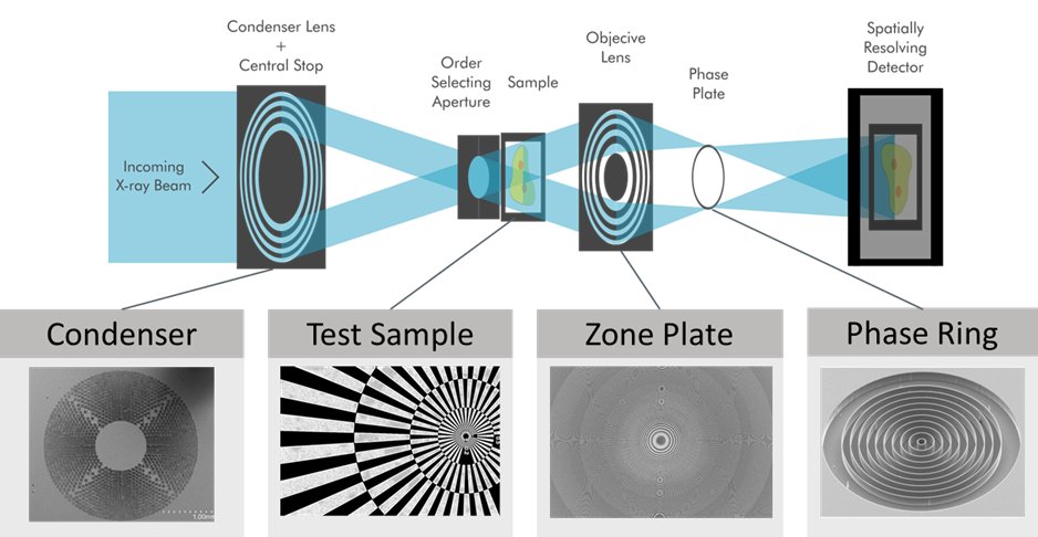
Full field transmission X-ray microscopy optical system with phase contrast imaging - Harmonized optical solution - Condensers, Fresnel zone plates and phase rings - Material choice: Au, Ir - High-resolution imaging All components included, such as beam-shaping condensers, Fresnel zone plates, and Zernike phase rings, working seamlessly together for an advanced and high resolution X-ray microscopy system. We optimize precision beam control and phase contrast with compatibility between the components to ensure efficient focusing, phase contrast enhancement, and beam shaping for high-clarity imaging
CATEGORY
