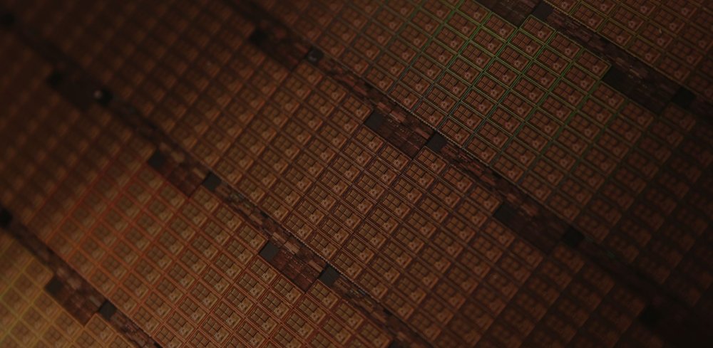
OptiStack® multilayer systems are our flagship lithography technology, and are used for leading-edge high volume IC manufacturing. OptiStack® multilayer lithography systems are designed for the most advanced high-volume semiconductor manufacturing processes in the world. Our versatile OptiStack® material set is designed to be used in combination with our proprietary optical modeling to achieve the finest resolutions possible with 193-nm immersion lithography. The OptiStack® system advantage - A universal substrate – OptiStack® materials work together to planarize a wide range of topography, effectively creating a "universal substrate" for advanced processes. - Superior optical performance – OptiStack® modeling systems work with unique paramaters to yield superior pattern fidelity to that of standard modeling systems. - High aspect ratio capabilities – OptiStack® materials maintain excellent pattern fidelity even at extreme aspect ratios. How OptiStack® multilayer systems work OptiStack® multilayer systems use a combination of a thick, carbon-rich underlayer, a thin silicon hardmask, and a thin photoresist to achieve accurate pattern transfer to the substrate. Some scenarios also require an additional bottom anti-reflective coating (BARC) beneath the photoresist. After the thin photoresist is imaged, the pattern is transferred to the silicon hard mask (Si-HM, also known as a spin-on glass or SOG) using a highly selective etching process, such as fluorinated plasma. The pattern is then transferred to the carbon-rich underlayer (known as a spin-on carbon or SOC) with another selective etching process, typically an oxygen-rich plasma. The imaged hardmask and SOC layers can then be used to transfer the pattern to the substrate. Why we need multilayer lithography systems Immersion lithography requires the photoresist to be extremely thin due to the shallow depth of focus inherent in high-NA optical systems. At these thicknesses, the photoresist can no longer survive the etching steps required to transfer the pattern into the substrate. The additional materials in a multilayer stack essentially work to magnify the etch resistance of the photoresist.
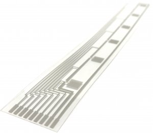
Temperature Sensor Arrays for FHE Applications Brewer Science can deliver highly sensitive, printed, metal temperature sensors for precise measurement of temperature on large areas and array applications. Temperature sensors can be used in a wide array of applications, enabling accurate, real-time responses to small changes in temperature. Our sensors provide full digital output with an onboard microcontroller for signal processing, have a flexible form factor, and can measure absolute temperature to within 1˚C. What Are RTDs? Resistive temperature detectors (RTDs) are devices that use resistance to show significant changes in temperature. These devices measure temperature by passing a low-level current through electrodes and measuring voltage drop across them. Why FHE Temperature Arrays? Flexible hybrid electronic (FHE) temperature arrays enhance many different applications and markets. Typically, users look for printed FHE systems when looking to measure temperature in confined spaces with narrow areas where typical silicon sensors can’t fit. FHE arrays are key for measuring multi-point surface temperature. Benefits of FHE Temperature Arrays - Full digital output with onboard microcontroller for signal processing - Flexible form factor - Measures absolute temperature to within 1˚C - Millisecond data capture for enhanced yield and throughput - Improves decision-making capabilities through real-time data collection - Easily interfaces to existing electronic systems to make fully printed temperature arrays for temperature monitoring in 2D surfaces - Able to be implemented into arrays for multi-point measurements, including different sensing technologies Potential Applications - Industrial tool optimization - Monitoring of electronic components - Environmental monitoring - Consumer applications - Batteries, displays, LEDs - Power supply - Electrical and hybrid vehicle batteries - Thermal mapping and imaging Specification Performance Parameters | Performance Resistance Value (at 25 ̊C) | 300 ± 10%Ω Accuracy: (-20˚C to +100˚C) | 0.6˚C Accuracy: (-40˚C to +120˚C) | 0.8˚C Operating Temperature | -40˚C to 120˚C Temperature sensors with higher operating temperature range (-50˚C, 250˚C) are also available When cycled from ambient to maximum temperature for a maximum 10 hours. We have found in our review of NIST standards for temperature sensors, drift at the upper temperature limit for an extended time (typically 10 hours)
CATEGORY
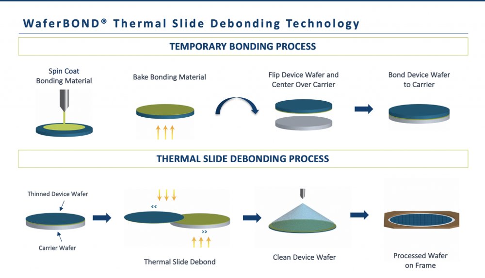
Temporary Bonding Material WaferBOND® HT-10.11 temporary bonding material enables back-end-of-line (BEOL) processing of ultrathin wafers with standard semiconductor equipment. WaferBOND® HT-10.11 material is an organic coating developed for temporary wafer bonding solutions for MEMS and 3-D wafer-level packaging applications. WaferBOND® HT-10.11 material enables effective bonding and support through substrate thinning and backside standard lithographic processing through the utilization of effective bonding and subsequent thermal slide, chemical, mechanical, or laser debonding for thickness < 75 μm. These materials were specifically developed for thin wafer handling (TWH), through-silicon via (TSV) reveal, and redistribution layer (RDL) creation or processes up to 250°C. Chemical release debond method requires a perforated carrier wafer or small die size if releasing after dicing Mechanical and laser debond methods require a compatible release material Wax Replacement WaferBOND® HT-10.11 material is an organic coating that enable back-end-of-line (BEOL) processing of ultrathin wafers using standard semiconductor equipment. This material is a great option as an alternative solution to typical wax adhesives. WaferBOND® HT-10.11 material offers significant advantages because it can be applied with a one-coat process, improve throughput, simplify cleaning, and shorten processing time. Properties | Wax | WaferBOND® HT-10.11 Material Thickness Range | ~ 10 – 35 µm | 20 µm – 130 µm Coating Throughput | Requires multiple coats | Single-coat process Bonding Temperature Range | 95°C – 110°C | 130°C – 180°C Debonding Temperature Range | 95°C – 110°C | 150°C – 200°C Thermal Stability Temperature Range | < 120°C | ≤ 250°C Benefits - Enables ultrathin wafer processing utilizing standard BEOL techniques and tooling - Assists in creation of interconnects (RDL layers) after thinning - Protect devices from chemical degradation and physical breakage - Adhesive materials can be completely removed from device wafer without damage - Can be utilized with various debond methods (chemical release, thermal slide, mechanical, or laser) Debond Methods WaferBOND® HT-10.11 material is compatible with the following debond methods: - Chemical Release System - Laser Release System - Mechanical Release System - Thermal Slide Release System With this WaferBOND® material, you can: - Process ultrathin wafers in temperatures up to 250°C - Protect the wafer edge from chipping - Protect circuitry from harsh chemical etchants - Provide a void-free interface for a smooth surface on the final thinned wafer WaferBOND® HT-10.11 Material Spin Speed Curve:
CATEGORY

Brewer Science is proud to offer an extensive program dedicated to exploring new realms of sensor performance – environmental monitoring. With decades of material science expertise, Brewer Science sensor solutions are designed to provide detailed, reliable data on key environmental parameters in a wide variety of applications. Brewer Science provides printed sensors for environmental monitoring to help your organization gather data that can increase safety, efficiency and performance of new and existing systems. We utilize unique materials to create application-specific printed sensors, allowing our device systems to provide accurate, ubiquitous monitoring. Brewer Science® InFlect™ printed sensors are reliable, low power, light weight and have flexible form factor. Customized electronics, seamless integration capabilities, and advanced software algorithms enable our systems to deliver real-time, actionable insight for the user. Sensing Capabilities - Flex - Gas - Humidity - Ion - pH - Temperature - Waste Water Benefits of Brewer Science Printed Sensors for Environmental Monitoring - Printed on flexible substrates to enable effortless integration - Differentiated customer experience via device customization & service support - Rapid detection of infrastructure failure & releases of hazardous products enable risk-informed management decisions - Provide systems of devices that can be integrated in almost any location that map diverse, real-time conditions - Able to be implemented into arrays for multi-point measurements, including different sensing technologies Applications - Air (Indoor & Outdoor) - Quality Monitoring - Residential - Water Monitoring (Ground, Surface, Water Supply & Industrial) - Soil Monitoring
CATEGORY
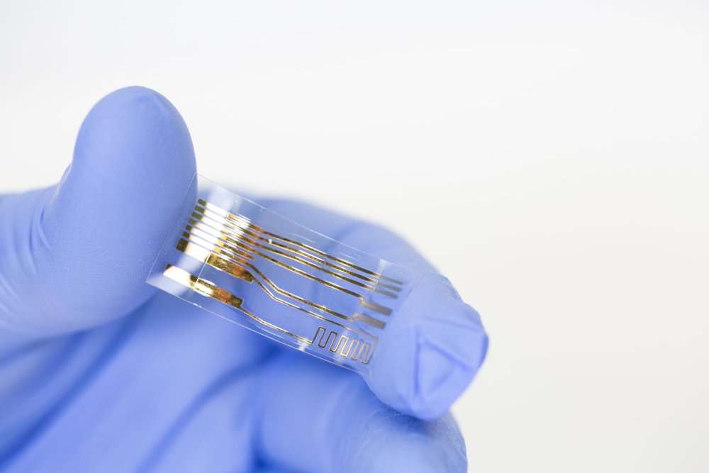
Real-time Water Quality Sensors Expect More From Your Water Real-time Water Quality Sensing Customized water sensor systems and devices, combined with unique materials and designs, enable viable resource monitoring for enhanced quality of life. Water quality sensors can be used in a wide array of applications such as water quality monitoring, resource optimization, and environmental monitoring. Our sensors provide full digital output with an onboard microcontroller for signal processing and can measure analytes such as lead, nitrates, conductivity, and pH. Current Methods are Slow and Cumbersome Today, water samples are collected manually and tested at a laboratory. Wait times for results are typically measured in weeks or longer. Testing systems are not modular, requiring multiple systems to test for additional parameters. All of this labor, time, and equipment increase the cost significantly. Brewer Science InFlect® water quality sensor systems offer enhanced efficiency and a simplified solution compared to current methods. Benefits - Arrays for multi-point measurements, including different sensing technologies - Improves decision-making capabilities through real-time data collection - Simple operation; automated sensing delivers results without manual input - Adaptive design for applications across many industries - Millisecond data capture for enhanced yield and throughput - Full digital output with onboard microcontroller for signal processing Applications - Water quality monitoring - Resource optimization - Condition monitoring - Process optimization - Environmental monitoring Detection Ranges Parameter | Range Lead (Pb 2+) | 1 to 10,000 ppb Nitrate (NO 3–) | 1 to 100 ppm Temperature | 1˚C to 40˚C pH | 4.5 to 10.5
CATEGORY
