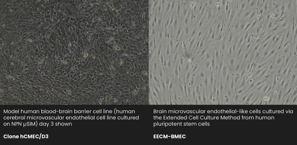
Microbubble Array™ products promote a wide range of research activities due to their unique features. - One-of-a-kind hemispherical microcavities within a cell-compatible substrate - Cavities with nanoliter volumes are ideal for creating microenvironments in which to culture and assay single-cell and multicellular spheroids and organoids - Useful for stem cell and antibody-producing cell clonal selections - Available in convenient Chamber Slide, Multi-Well plate, and Culture Dish formats with various cavity opening and volume sizes MB arrays can be used to identify drug-resistant cancer cells. MC-1 is a melanoma cancer cell line derived from lung metastasis. MC-1s grown in a hydrophobic environment displayed a nonadherent phenotype. Images of MC-1 melanoma cells cultures after 48 hours in increasing Cisplatin treatment. Live cells are stained with green Calcein-AM.

3×3 windows 2.9 mm diameter/hexagonal + 0.1 mm thick Sold in packs of 10 US100H-A05Q33A $506.40 Only 10 left! (can be backordered) Material: Amorphous Silicon | Thickness: 5 nm | Porosity: N/A | Window Size: (8) 50x50 µm + (1) 50x100 µm | Chip Frame: 2.9 mm hexagonal + 0.1 mm thick US100H-A09Q33 $506.40 32 available (can be backordered) Material: Amorphous Silicon | Thickness: 9 nm | Porosity: N/A | Window Size: (8) 100x100 µm + (1) 100x350 µm | Chip Frame: 2.9 mm hexagonal + 0.1 mm thick US100H-A15Q33 $506.40 17 available (can be backordered) Material: Amorphous Silicon | Thickness: 15 nm | Porosity: N/A | Window Size: (8) 100x100 µm + (1) 100x350 µm | Chip Frame: 2.9 mm hexagonal + 0.1 mm thick US100H-C25Q33A $506.40 Out of stock Material: Single-crystal (1-0-0) Silicon | Thickness: 25 nm | Porosity: N/A | Window Size: (8) 50x50 µm + (1) 50x100 µm | Chip Frame: 2.9 mm hexagonal + 0.1 mm thick Material: Amorphous Silicon, Single-crystal (1-0-0) Silicon Thickness: 5 nm, 9 nm, 15 nm, 25 nm Porosity: N/A Window Size: (8) 50×50 µm + (1) 50×100 µm, (8) 100×100 µm + (1) 100×350 µm Chip Frame: 2.9 mm hexagonal + 0.1 mm thick Primary Application: Electron Microscopy Secondary Applications: High-resolution EM, Sample Deposition
CATEGORY
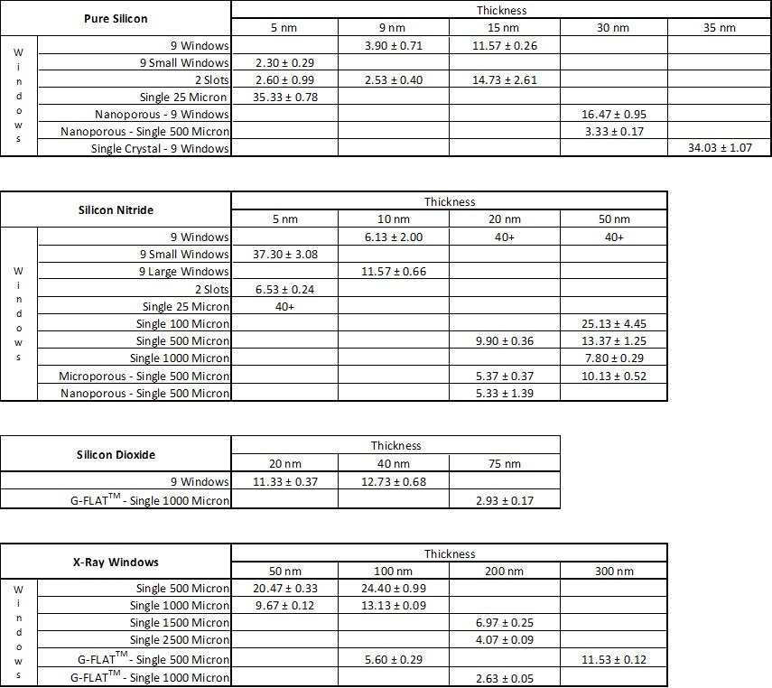
Product Information Sheet: Differential pressure tolerance for TEM and X-Ray Window membranes by thickness and size All our membrane types and membrane area configurations have been robustness tested by application of differential pressure. In these tests, the membrane was oriented such that differential pressure forced the membrane against the chip frame. In the opposite orientation where the membrane would be delaminated from the chip frame, the pressure tolerance would be several times lower. All values below are the maximum tolerated differential pressure reported as mean +/- standard deviation (n = 3), in units of PSI. Window Sizes: - 9 Windows: (8) 100×100, (1) 100×350 micron - 9 Small Windows: (8) 50×50, (1) 50×350 micron - 2 Slots: (2) 50×1500 micron - Single Windows: (1) square window of x micronside-length
CATEGORY

Sold in packs of 10 Material: Amorphous Silicon | Thickness: 5 nm | Porosity: N/A | Window Size: (2) 50x1,500 µm | Chip Frame: 2.9 mm hexagonal + 0.1 mm thick Material: Amorphous Silicon | Thickness: 9 nm | Porosity: N/A | Window Size: (2) 100x1,500 µm | Chip Frame: 2.9 mm hexagonal + 0.1 mm thick Material: Amorphous Silicon | Thickness: 15 nm | Porosity: N/A | Window Size: (2) 100x1,500 µm | Chip Frame: 2.9 mm hexagonal + 0.1 mm thick Material: Amorphous Silicon Thickness: 5 nm, 9 nm, 15 nm Porosity: N/A Window Size: (2) 50×1,500 µm, (2) 100×1,500 µm Chip Frame: 2.9 mm hexagonal + 0.1 mm thick Primary Application: Electron Microscopy Secondary Applications: High-resolution EM, Sample Deposition
CATEGORY
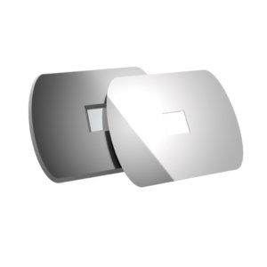
APT100-Q05 $149.20 Only 4 left! Material: Silicon |Window Size: (1) 500 µm |Chip Frame: 2.9 mm diameter + 0.1 mm thick APT100-Q01 $149.20 32 available Material: Silicon |Window Size: (1) 100um |Chip Frame: 2.9 mm diameter + 0.1 mm thick Chip frame: 2.9 mm diameter/hexagonal + 0.1 mm thick Sold in packs of 10 SKU: TEM-APT Material: Silicon Window Size: (1) 100um, (1) 25 µm, (1) 50 µm, (1) 500 µm Chip Frame: 2.9 mm diameter + 0.1 mm thick, 2.9 mm hexagonal + 0.1 mm thick Primary Application: Electron Microscopy Secondary Applications: FIB Sample Preparation, High-resolution EM, Sample Deposition
CATEGORY
