By NanoIntegris Technologies, Inc.
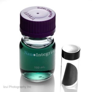
Metallic SWNTs Overview Diameter Range 1.2nm-1.7nm Length Range 300 nm to 5 microns Solution Color Green Metal Catlyst Impurity<1% Amorphous Carbon Impurity 1-5% Electronic Enrichment 70%, 90%, 95%, 98%, 99% Product Applications The IsoNanotubes-M product has been a reliable staple of NanoIntegris Technologies for many years now. This one-of-a-kind, high-purity, conductive material can be utilized fir many types of applications such as a replacement for Indium Tin Oxide (ITO) in flexible electronics, within highly conductive wire composites, smart glass/ windows, within high-speed bolometers for Infrared sensors, and for developing intelligent cellular delivery systems. High Speed Bolometers Work performed at the Center for Future Energy Systems, Rensselaer Polytechnic Institute has shown the metallic IsoNanotubes are a suitable material for infrared sensors; specifically for application to microbolometers. It was found that highly cracked composites containing IsoNanotubes-M had the best properties over other nanotubes. Measurements of Temperature Coefficient of Resistance (TCR) was -6.7%/K at 25˚C, Device Responsivity: 62 V/W @ 500mV bias, Film conductivity of 1.69×10⁻⁶ S/m, and a Time constant of ~560 µs at 63% response. Proc. of SPIE Vol. 8632 863205-2 siRNA Nuclear Localization Research by scientists at University of Waterloo School of Pharmacy have found that complexes created with IsoNanotubes-M material may be a great prospect for developing intelligent cellular devlivery systems, targeting particular nuclei. Some of the wonderful properties found were 1 hr binding of SWNT complex to cellular membranes followed by subsequent uptake into cytoplasm, with higher selectivity toward nucleoli, as compared to semiconducting or un-electronically separated nanotube sources. Future Sci. OA (2015) FSO17 Highly Conductive Wire Composites At the NASA Glenn Research Center, Dr. Henry C. de Groh III was able to create a Copper Carbon Nanotubes Composite 1, utilizing the IsoNanotubes-M 95% material displaying enhanced conductivity of +246%, as compared to unsorted nanotubes. It was also theorized that such composites will lead to wires with enhanced current carrying capacity (amapacity) over long lengths. [1] MRS Advances, Volume 2, Issue 2 (Nanomaterials)2017, pp. 71-76 Product Delivery We currently offer our nanotube products in two forms: Aqueous surfactant solution and surfactant-eliminated “powder” (thick film or buckey paper). We remove the surfactant from our powders via a proprietary process that involves filtration and rinsing. The end result is a film-like structure, as can be seen in the above picture, bearing a density around 1mg/ 4.8cm 2. Our powders have been formulated so that they are easy to use, break apart, and disperse in solvents with gentle sonication. Prices Multi-gram and kilogram price quotes available by request. Additional discounts also available for large volume orders. To place an order contact our Sales Manager at sales@nanointegris.com or call +1-866-650-0482. Metallic Purity | Solution ($ USD) | Thick Film ($ USD) 1mg, 99% | $1050 | $1100 2mg, 98% | $1600 | $1700 3mg, 95% | $1600 | $1700
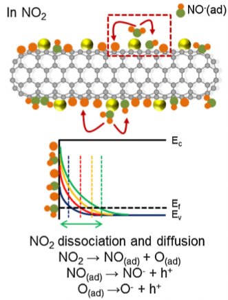
Semiconducting SWNT’s Overview FE-SEM of IsoNanotubes-S Thick Film Image by Najia Mahdi of NORCADA Diameter Range 1.2nm-1.7nm Length Range 300 nm to 5 microns Solution Color Light Crimson/ Pink Metal Catlyst Impurity<1% Amorphous Carbon Impurity 1-5% Electronic Enrichment 90%, 95%, 98%, 99%, and 99.9% Product Applications The IsoNanotubes-Semiconducting product has been successfully utilized in numerous scientific works over the years. The primary usage for the IsoNanotubes-S material is for the creation of thin film transistors. Because of the IsoNanotubes-S’ high single-walled nanotube purity, length, pristine surface, and semiconducting properties, this material has proven beneficial in applications such as Gas Detection, Temperature Sensing, CMOS circuit creation, and has laid the ground work for the development of novel and exciting technological advancements. Temperature Sensing/ Wearable Devices Mechanically flexible CMOS digital and analog circuits were fabricated on a polyimide substrate by monolithic ingegration of n-type TFTs, p-type CNT-TFTs, and a temperature sensor made of CNTs and PEDOT:PSS, with the CNT source being NanoIntegris’ IsoNanotubes-S 99% solution. [1] The following electrical properties of the CNT-TFTs were found: field-effect mobility of 9.95 ±2.08cm 2 V-1 s-1, on-current (I on)/off-current (I off) ratio (Log I on/I off) of 4.65 ±0.70V and threshold votage of -1.63 ±0.24V. The flexible CMOS J-K flip flop digital circuit was also found to a memory function demonstrated when 5 or 0 Volts were applied to the J and K inputs. When operated, the power consumption at steady state was ~68.7nW/mm and 6.34 µW/mm with an applied CLK signal. It was also found that the electrical properties remained unchanged (no malfunction or TFT leakage) with a bending radius of 5.6mm and 500 bending cylces. Additionally, analog circuits were fabricated in the form of a differential amplifier. The circuit produced a peak gain of ~31.7dB, corresponding to a 38.5 times amplification. This amplified was utilized to fabricate a temperature sensor in which the electrical resistance was decreased with increasing temperature. In the temperature range of 28 and 34°C, the rate of voltage change was found to be 0.4V/°C when using the amplifier, with a range that can be tuned by changing the input voltage. Such an approach can used for creating wearable devices for monitoring skin temperature. [1] Adv. Mater. Technol. 2016, 1, 1600058. Gas Detection Members of the Sensor System Research Center at the Korea Institute of Science and Technology have created a highly sensitive gas detector by using platinum nanoparticles decorated with NanoIntegris’ IsoNanotubes-S 99% single-walled carbon nanotubes. [1] These sensors were able to detect numerous gases such as NO2, NO, C6H6, C7H8, C3H6O, CO, and NH3 but proved the most successful in the detection of nitrogen dioxide (NO2) at sensitivities down to 2ppm. It was also greatly promising to find that the sensors showed almost complete recovery (~95%) and facilitated both chemisorption and dissociation of NO2 molecules. [1] Sensors and Actuators B 238 (2017) 1032-1042. Product Delivery We currently offer our nanotube products in two forms: Aqueous surfactant solution and surfactant-eliminated “powder” (thick film or buckey paper). We remove the surfactant from our powders via a proprietary process that involves filtration and rinsing. The end result is a film-like structure, as can be seen in the above picture, bearing a density around 1mg/ 4.8cm 2. Our powders have been formulated so that they are easy to use, break apart, and disperse in solvents with gentle sonication. Prices Multi-gram and kilogram price quotes available by request. Additional discounts also available for large volume orders. To place an order contact our Sales Manager at sales@nanointegris.com or call +1-866-650-0482. Product Purity | Solution ($ USD) | Thick Film ($ USD) 1mg, 99.9% | $1050 | $1100 1mg, 99% | $945 | $995 2mg, 98% | $1050 | $1150 3mg, 95% | $1050 | $1150
CATEGORY
Our PureWave Graphene Nanoplatelets (GNP) material is composed of thin, highly dispersible 4-7 layer graphene nanoplatelets with very low oxygen and polyaromatic hydrocarbon (PAH) content. The turbostratic and wavy morphology of the material leads to an unequaled ability to be dispersed in a variety of solvents and resins. Furthermore, the unique plasma process used to grow our PureWave Graphene Nanoplatelets is easy to scale and thus produces a low cost, but high-quality product. Our unique and patent-protected growth process, based on inductively-coupled plasma, allows us to produce this material at over 100 g/hour, enabling commercial graphene applications such as energy storage and conductive inks as well as elastomers and resins. Using our special milling process, our PureWave Graphene nanoplatelet powder can be effectively dispersed into a water-soluble polymer matrix. This allows for the creation of a material with very advantageous properties at high loadings (up to 8 wt% Graphene) that can be utilized for numerous applications to provide thermal stability, mechanical property enhancement, dielectric constant improvement, and electrical conductivity. We currently offer our graphene product as a fine, fluffy powder which can be easily dispersed into numerous solvents and colloidal suspensions. Additionally, the product is offered as a liquid dispersion into a proprietary solvent system. SKU 1710 | Quantity (g) 10 | Powder (USD) $1150 | Dispersion (USD) $1950 Kilogram and metric ton price quotes available by request. Additional discounts also available for large volume orders. ONLINE SHIPPING CHARGES International (Asia, Europe, India): $100.00 United States: $50 Canada: $30
CATEGORY
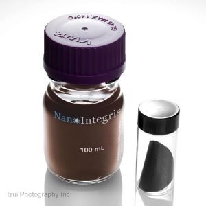
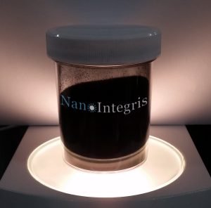
Unseparated SWCNTs FE-SEM's OF SUPER PURETUBES THICK FILM Diameter Range 1.2nm-1.7nm Length Range 300 nm to 5 microns Solution Color Dark Brown/ Gray Metal Catlyst Impurity<1-3.5% Amorphous Carbon Impurity 1-5% Download: Technical Specifications Sheet Solution: Safety Data Sheet Thick Film: Safety Data Sheet We currently offer our nanotube products in two forms: Aqueous surfactant solution and surfactant-eliminated "powder" (thick film or bucky paper). We remove the surfactant from our powders via a proprietary process that involves filtration and rinsing. The end result is a film-like structure, as can be seen in the above picture. Our powders have been formulated so that they are easy to use, break apart, and disperse in solvents with gentle sonication. Multi-gram and kilogram price quotes available by request. Additional discounts also available for large volume orders. Type: Super PureTubes; Metal Catalyst Impurities: <1.0%; Solution (100mg): $1155; Thick Film (75mg): $945 ONLINE SHIPPING CHARGES International (Asia, Europe, India): $100.00 United States: $50 Canada: $30
CATEGORY
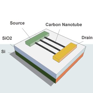
Semiconducting carbon nanotubes may replace or complement traditional semiconductors in both high-performance and low-cost thin film transistor (TFT) devices. IBM and the University of Southern California have used our IsoNanotubes-S carbon nanotubes to create TFTs with the best concurrent on/off ratios and on-drive currents reported in the literature to date. When used as a local back gate our high-density single walled carbon nanotube thin films were used as an effective Field-Effect Transistor when on an amino-silane-treated hafnium oxide (HfOX) surface.
CATEGORY
