By Smoltek
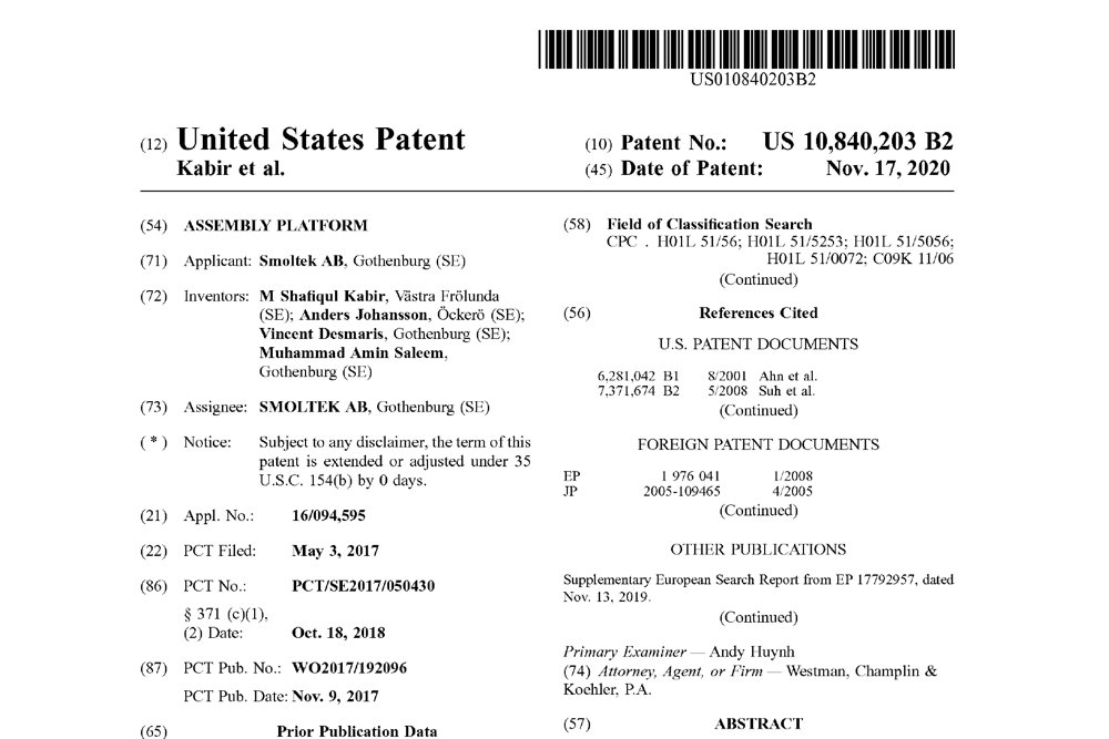
The Assembly platform family is a particular application in the field of interconnects and heterogeneous integration. The invention: An assembly platform for arrangement as an interposer device between an integrated circuit and a substrate to interconnect the integrated circuit and the substrate through the assembly platform, the assembly platform comprising: an assembly substrate; a plurality of conducting vias extending through the assembly substrate; at least one nanostructure connection bump on a first side of the assembly substrate, the nanostructure connection bump being conductively connected to the vias and defining connection locations for connection with at least one of the integrated circuit and the substrate, wherein each of the nanostructure connection bumps comprises: a plurality of elongated conductive nanostructures vertically grown on the first side of the assembly substrate, wherein the plurality of elongated nanostructures are embedded in a metal for the connection with at least one of the integrated circuit and the substrate, at least one connection bump on a second side of the assembly substrate, the second side being opposite to the first side, the connection bump being conductively connected to the vias and defining connection locations for connection with at least one of the integrated circuit and the substrate.

Smoltek Semi develops ultra-thin high-performance capacitors for AI and advanced electronics. The semiconductor market for these types of capacitors is rapidly increasing, driven by the need for higher capacitance density and superior high-frequency performance. Smoltek's CNF-MIM technology combines high capacitance density and low parasitic inductance with ultra-compact form factor delivered on various substrates. By using a single dielectric stack for capacitor manufacturing Smoltek enables efficient power management for AI, High-Performance Computing, and premium electronics at lower production costs. The most demanding electronic applications require next-generation, ultra-thin capacitors that deliver high capacitance density, exceptional high-frequency performance, robust temperature stability, and very low losses. Smoltek Semi provides the foundational technology to meet these demands. We use carbon nanofibers (CNFs) to create an immense 3D surface for metal-insulator-metal (MIM) capacitors. Unlike DTC, our process works on more than just silicon and uses only a single dielectric stack, increasing flexibility while reducing manufacturing complexity and cost. These features make our CNF-MIM technology an ideal solution for the world's most demanding applications. High capacitance density: The first generation of our capacitors, the "CNF-MIM Gen-One," has a target capacitance density of 250 nF/mm². In future generations we aim to exceed 1,500 nF/mm² in an ultra-thin profile. High frequency: Engineered for high-speed systems, our capacitors ensure stable power delivery to advanced processors. With exceptionally low inductance (ESL < 2 pH) and resistance (ESR < 50 mΩ), they are a key advantage for power integrity. Low losses: Our capacitors ensure power is used effectively, with an ultra-low leakage current of less than 100 pA at 2 V and minimal resistive losses. This superior efficiency is crucial for extending battery life in compact, power-sensitive devices. Temperature stability: We deliver reliable performance, guaranteeing stability for demanding applications. Our technology shows only a ~2.5% capacitance change when tested up to 125°C, ensuring your system performs as designed across wide temperature ranges. We have demonstrated 1 µF/mm² (1,000 nF/mm²) capacitance density with an active layer thickness of just 6 µm. This combination of high capacitance and ultra-thin profile makes the technology suitable for under-chip integration where height constraints are critical. Prototypes using our advanced high dielectric stack have passed temperature and voltage stress testing.
CATEGORY
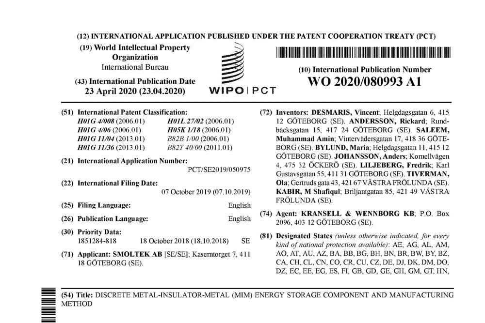
The Discrete CNF-MIM patent family is covering a method for manufacturing of discrete capacitor components based on our CNF-MIM technology. The innovation exploits the extra-ordinary surface to volume ratio provided by carbon nanofibers to create a MIM capacitor with unparalleled high capacitance density. S Kabir, A Johansson, A M Saleem, R Andersson, V Desmaris, Fredrik Liljeberg, O Tiverman • June 13, 2023 The invention: A discrete two-terminal metal-insulator-metal (MIM) capacitor component, the capacitor component comprising: a MIM-arrangement comprising: a first electrode layer; a plurality of conductive nanostructures grown from the first electrode layer; a solid dielectric material layer conformally coating each nanostructure in the plurality of conductive nanostructures and the first electrode layer uncovered by the conductive nanostructures; and a second electrode layer covering the solid dielectric material layer a first connecting structure for external electrical connection of the capacitor component a second connecting structure for external electrical connection of the capacitor component; and an electrically insulating encapsulation material at least partly embedding the MIM-arrangement.
CATEGORY
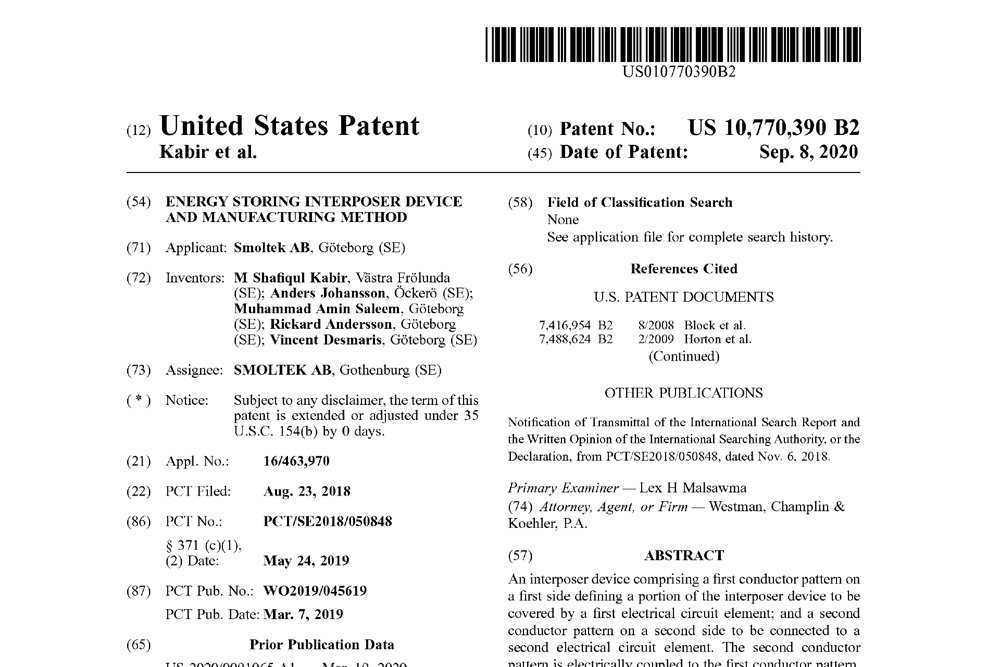
The Compact Energy Storage Interposer family is covering the invention and manufacturing of extremely thin energy storage devices embedded in an interposer. The invention: An interposer device comprising a first conductor pattern on a first side defining a portion of the interposer device to be covered by a first electrical circuit element; and a second conductor pattern on a second side to be connected to a second electrical circuit element. The second conductor pattern is electrically coupled to the first conductor pattern. The interposer device further comprises a plurality of nanostructure energy storage devices arranged within the portion of the interposer device to be covered by the first electrical circuit element. Each of the nanostructure energy storage devices comprises at least a first plurality of conductive nanostructures; a conduction controlling material embedding the nanostructures; a first electrode connected to each nanostructure in the first plurality of nanostructures; and a second electrode separated from each nanostructure in the first plurality of nanostructures by the conduction controlling material. Granted patents relating to the innovation - India: IN321032 - South Korea: KR102059450 - South Korea: KR102340123 - USA: US10770390 - USA: US10991652 - Taiwan: I766072 For more information about a particular patent, click on its name to view it on Google Patents.
CATEGORY
