By PiezoDrive
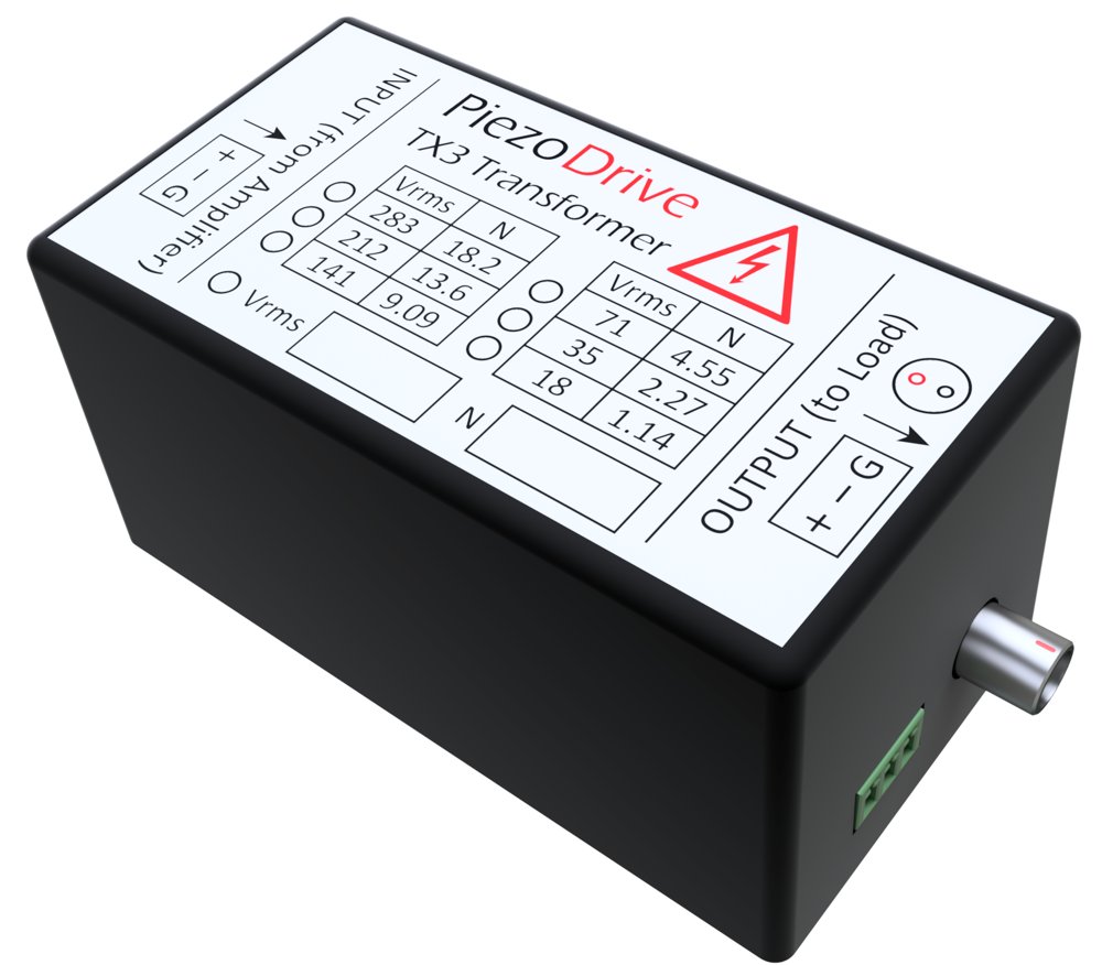
Turns Ratio 3.98, Voltage pk-pk 175, Voltage RMS 62, Amps pk-pk 9.1, Amps RMS 3.2, Optimal Load Ohms 19.1, Load Range Ohms 12 - 40, Frequency kHz 10-100
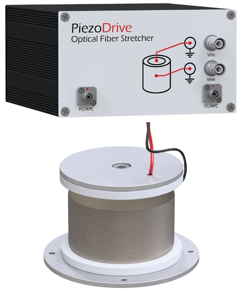
The FS Optical Fiber Stretcher is a highly customizable optic fiber stretcher based on a piezoelectric tube actuator. The selected fiber is wound onto the tube with a controlled tension. During operation, a voltage applied to the piezoelectric tube results in a change in diameter and a proportional change in the optical path length. Customizations include the fiber type, number of turns, optical connection type, and electrical drive configuration. Single-mode (SM) and polarization-maintaining (PM) fibers are available. The PiezoDrive FS Optical Fiber Stretcher can be purchased in an enclosure or as an OEM component with no enclosure. The enclosed option uses two FC/APC optical connectors and has two electrical configurations available. The two electrical configuration options are single-ended, and differential. The simplest option is the single-ended connection, where the external tube surface is grounded, and only the internal tube electrode is driven, which requires one high-voltage amplifier. Alternatively, the differential option has electrical connections to both the internal and external tube electrodes, which requires two high-voltage amplifiers. The differential configuration may be suitable for some applications that require maximum bandwidth or displacement range, since the voltage and power requirements of each high-voltage amplifier are halved. The enclosed version can be supplied with BNC or SHV electrical connectors. Applications include variable optical delays, interferometers, laser stabilization, and laser tuning. Electrical Specifications Maximum Input Voltage: -500 to +2000 V (Dependent on connector type and configuration) Tube Capacitance: 289 nF Electrical Connections: BNC or SHV Wavelength Range: 320 to 2100 nm (Dependent on fiber choice) Optical Path Displacement Sensitivity: 36 nm/V/turn (Dependent on the number of fiber turns) Number Of Turns: 1, 5, 10, 15… 80 Total Fiber Length: 300 mm + 180 mm/turn (Dependent on the number of fiber turns) Resonance Frequency: 14 kHz Fiber Type: SM or PM Optical Connectors: FC/APC Optical Connectors (OEM): Custom Single Mode Fibers SM300: 0.13 NA; 320 – 430 nm; Cladding: 125 um S405-XP: 0.12 NA; 400 – 680 nm; Cladding: 125 um SM450: 0.12 NA; 488 – 633 nm; Cladding: 125 um 460HP: 0.13 NA; 450 – 600 nm; Cladding: 125 um SM600: 0.13 NA; 633 – 780 nm; Cladding: 125 um SM400: 0.13 NA; 405 – 532 nm; Cladding: 125 um 630HP: 0.13 NA; 600 – 770 nm; Cladding: 125 um S630-HP: 0.13 NA; 630 – 860 nm; Cladding: 125 um 780HP: 0.13 NA; 780 – 970 nm; Cladding: 125 um SM800-5.6-125: 0.13 NA; 830 nm; Cladding: 125 um SM800G80: 0.16 NA; 830 nm; Cladding: 80 um SM980-5.8-125: 0.14 NA; 970 – 1650 nm; Cladding: 125 um SM980G80: 0.18 NA; 980 – 1650 nm; Cladding: 80 um 1060XP: 0.14 NA; 980 – 1600 nm; Cladding: 125 um 980HP: 0.2 NA; 980 – 1600 nm; Cladding: 125 um 1310BHP: 0.13 NA; 1300 – 1625 nm; Cladding: 125 um SM1250G80: 0.12 NA; 1310 – 1550 nm; Cladding: 80 um SM2000: 0.11 NA; 1700 – 2100 nm; Cladding: 125 um UHNA1: 0.28 NA; 1100 – 1600 nm; Cladding: 125 um UHNA3: 0.35 NA; 960 – 1600 nm; Cladding: 125 um UHNA4: 0.35 NA; 1100 – 1600 nm; Cladding: 125 um DCF13: 0.12 NA; 1250 – 1600 nm; Cladding: 125 um DCF4: 0.11 NA; 1500 – 1625 nm; Cladding: 125 um Polarization Maintaining Fibers PM-S350-HP: 0.12 NA; 350 – 460 nm; Cladding: 125 um PM-S405-XP: 0.12 NA; 400 – 680 nm; Cladding: 125 um PM460-HP: 0.12 NA; 460 – 700 nm; Cladding: 125 um 460HP: 0.13 NA; 450 – 600 nm; Cladding: 125 um PM630-HP: 0.11 NA; 620 – 850 nm; Cladding: 125 um PM780-HP: 0.12 NA; 770 – 1100 nm; Cladding: 125 um PM980-XP: 0.12 NA; 970 – 1550 nm; Cladding: 125 um PM1300-XP: 0.12 NA; 1270 – 1625 nm; Cladding: 125 um PM1550-XP: 0.13 NA; 1440 – 1625 nm; Cladding: 125 um PM2000: 0.2 NA; 1850 – 2200 nm; Cladding: 125 um PS-PM980: 0.12 NA; 980 nm; Cladding: 125 um HB830Z: 0.14 NA; 780 – 850 nm; Cladding: 80 um HB1060Z: 0.14 NA; 1014 – 1114 nm; Cladding: 125 um HB1550Z: 0.09 – 0.11 NA; 1500 nm; Cladding: 125 um HB800G: 0.16 NA; 830 nm; Cladding: 80 um HB980T: 0.14 NA; 980 nm; Cladding: 125 um HB1250T: 0.12 NA; 1310 nm; Cladding: 125 um HB1500T: 0.12 NA; 1550 nm; Cladding: 125 um Optical Connectors For OEM FC/PC: FC/PC FC/APC: FC/APC LC/PC: LC/PC SC/PC: SC/PC ST: ST SMA: SMA LC/SSF: 1.25 mm (LC) Stainless Steel Ferrule LC/CF: 1.25 mm (LC) Ceramic Ferrule FC/SSF: 2.5 mm (FC) Stainless Steel Ferrule FC/CF: 2.5 mm (FC) Ceramic Ferrule SMA/N: SMA with Hex Nut Mechanical Specifications Enclosure Dimensions: 171 x 153 x 90 mm L x W x H OEM Dimensions: 90 x 90 x 52 mm L x W x H Humidity: Non-condensing Choosing Number of Turns The PiezoDrive FS Optical Fiber Stretcher allows for high customization. A key parameter that can be adjusted is the optical path displacement (OPD) sensitivity, which can be adjusted by changing the number of fiber turns. The ideal number of turns is determined by the available voltage range and the required change in path length. To simplify the choice of turns and driver, an online tool is available below. Alternatively, please contact advice and configuration inquiries. The configuration tool requires that you provide the required displacement and bandwidth needed for your application. Additionally, your signal source’s effective number of bits can be provided, allowing the tool to estimate the fiber stretcher’s resolution. OEM Option without Enclosure For OEM applications, the fiber stretcher can be supplied as a component without the enclosure and electrical connectors. It is recommended to use the online part builder to configure this; however, a part number can also be generated using the process described in the following section. The piezoelectric tube is also available as a stand-alone component (FS-TubeOnly) or mounted with wiring but without fiber (FS-OEM). OEM Version Without Enclosure or Electrical Connectors Ordering The FS Optical Fiber Stretcher can be ordered online, or you can download a quote using the same process. Please read the instructions for “Obtain Instant Quote” at the top of this page. You can also request a quote by submitting a support request. The PiezoDrive FS Optical Fiber Stretcher has the following order code format: FS-(Fiber Type)–(Fiber Order Code)-N(Number of Turns)–(Enclosure)–(Optical Connector 1)–(Optical Connector 2)–(Electrical Configuration) Fiber Type: SM or PM Fiber Order Code: see SM and PM fiber tables Number of Turns: number of fiber winds around the tube Enclosure: OEM for no enclosure, or ENCL for metal enclosure with mounted connectors Optical Connector 1/Optical Connector 2: blank for the enclosure option or see optical connector table Electrical Configuration: blank for OEM option or see the electrical configurations table Example 1: Fiber stretcher with no enclosure (OEM option) with 35 turns of SM300 single-mode fiber using FC/APC connectors: FS-SM-SM300-N35-OEM-FC/APC-FC/APC Example 2: 70 turns of 460HP polarization-maintaining fiber, in a an enclosure with a single-ended BNC electrical connector. FS-PM-460HP-N70-ENCL-BNCSGL Standard Delivery Contents - PiezoDrive FS Optical Fiber Stretcher (in chosen configuration) Certifications - Download CE, RoHS, and REACH statement. Warranty and Service The PiezoDrive FS Optical Fiber Stretcher is guaranteed against manufacturing defects for 12 months from the date of purchase. For service and support, contact your distributor or submit a support request. Please include the serial number.
CATEGORY
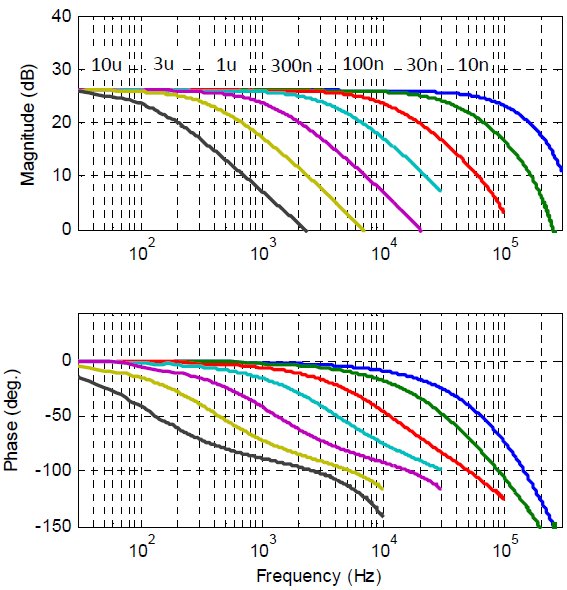
The PDu150 is a complete miniaturized power supply and ultra-low noise driver for up to three 100V, 120V or 150V piezoelectric stack actuators. Output currents up to 100mA per channel are developed at frequencies up to 80 kHz with very low noise. With a capacitive load, the peak-to-peak resolution exceeds one part-per-million or 20-bit, which suits demanding applications in semiconductor machinery, scanning probe microscopy, optics, vibration control, and nanopositioning. The PDu150 is protected against short-circuit, average current overload, and excessive temperature. Passive cooling is available for low power applications or the integrated fan can be used for power dissipations above 5W. The PDu150 can be mounted with four M2.5 screws. The PCB mounting version (PDu150-PCB) is supplied with headers for direct mounting onto a host motherboard. Specifications Power Supply +24 V (+/-10%) Output Voltage -30 V to +150 V Peak Current 100 mA (300 mA single channel) RMS Current 78 mA (235 mA single channel) Power Bandwidth 80 kHz (150 Vp-p) Signal Bandwidth 180 kHz Slew Rate 38 V/us Gain 20 V/V Input Impedance 9.16 kOhm (Input), 3.3 kOhm (Offset) Input Offset +/- 5 mV Load Unlimited Output Noise 26 uV RMS (1 uF load, 0.03 Hz to 1 MHz) Protection Short circuit, over-current, and temperature Quiescent Current 100 mA (10 mA in shutdown) Connectors Screw terminals (AWG 20-30) Dimensions 76 x 40 x 44 mm (L x W x H) Environment 0C to 60C (32F to 140F) Weight 80 gram Connection Diagram Pin Function G Ground EN Enable OS Offset R- -2V Reference R+ +10V Reference Operation The amplifiers have differential inputs where the negative input can be connected to an external reference or the internal offset generator. A precision +10V and -2V reference voltage (R+ and R-) are provided to allow external potentiometers to generate the amplifier inputs. The amplifier outputs use a novel low-noise differential architecture that cannot be connected to ground, for example, to the ground lead of an earthed oscilloscope. Offset Voltage Configuration The offset voltage can be set from either the internal potentiometer or by an external source by configuring the jumper LK1 to either "Internal" or "External". When using the internal offset source, the offset voltage is set by connecting a multimeter across the output and varying the potentiometer until the desired offset is obtained. In the external offset mode, the offset voltage is determined by the voltage applied to the OS pin. The offset voltage can be set to zero by grounding the OS pin, which is the standard configuration. Using the Reference Voltages A precision +10V and -2V reference voltage (R+ and R-) is provided to allow an external potentiometer to generate the amplifier input. Multiple potentiometers can be used for multiple channels. The 10uF capacitor reduces the noise bandwidth but is not strictly necessary. The capacitor should preferably be a film type but ceramic is acceptable in most applications. Output Current The peak output current is 100mA per channel, and the maximum average current is 35mA per channel. The average current is useful for calculating the power dissipation and average supply current. Supply Current The quiescent power for the amplifier is approximately 2 W or 85 mA. This can be reduced to <10 mA by pulling the Enable pin low with an open collector circuit. If the fan is used, the quiescent power is increased by 0.5W. The maximum supply current is 0.9A at full power. Power Bandwidth The power bandwidth is the maximum frequency periodic signal that can be reproduced without distortion. The calculator determines the maximum operating frequency and required power for a given load capacitance. The calculator includes the effects of current limit, slew-rate, output impedance, and signal bandwidth. The calculator does not include the time-constant of the peak current limit, and may be inaccurate when the power bandwidth is below 100 Hz. The nominal slew-rate of the PDu150 is 38 V/us. With a capacitive load, the power bandwidth is limited by the output current. Note that when all channels are connected in parallel, the output current and power bandwidth are tripled. Small Signal Bandwidth Load Capacitance / Bandwidth No Load 180 kHz 10 nF 105 kHz 30 nF 40 kHz 100 nF 11 kHz 300 nF 3.8 kHz 1 uF 1.0 kHz 3 uF 320 Hz 10 uF 62 Hz 30 uF 24 Hz Small Signal Bandwidth (-3dB) Noise The output noise contains a low frequency component (0.03 Hz to 10 Hz) that is independent of the load capacitance; and a high frequency component (10 Hz to 1 MHz) that is inversely related to the load capacitance. Optimal noise performance is achieved with passive cooling as magnetic fields from the fan can induce mV level interference in the outputs. In low noise applications, where the fan is removed, some external air-flow is required if the power dissipation is above 5W. The low frequency noise is measured with an SR560 low-noise amplifier (Gain = 1000), oscilloscope, and Agilent 34461A Voltmeter. The RMS value is 15 uV with a peak-to-peak voltage of 100 uV. The high frequency noise (10 Hz to 1 MHz) is listed versus load capacitance. The total noise from 0.03 Hz to 1 MHz can be found by square summing the RMS values. Load Capacitance / HF Noise RMS / Total Noise RMS 10 nF 450 uV 450 uV 30 nF 170 uV 171 uV 100 nF 60 uV 62 uV 300 nF 34 uV 37 uV 1 uF 21 uV 26 uV 3 uF 16 uV 23 uV 10 uF 16 uV 22 uV 30 uF 18 uV 23 uV High Frequency Noise (10 Hz to 1 MHz) and Total Noise (0.03 Hz to 1 MHz) Overload Protection / Shutdown The PDu150 is protected against short-circuit and average current overload. The amplifier can be shutdown manually by pulling the Enable pin low with an open-collector, or open-drain circuit. The Enable pin normally floats at 5V and should not be driven directly. Heat Dissipation A straight-forward method for measuring heat-dissipation is to measure the supply current with a multimeter during operation. The heat dissipation is equal to the product of DC current and voltage. In low-noise and low-power applications where it is desirable to remove the fan, natural convection is sufficient if the heat dissipation is less than 5W. If the heat dissipation is above 5W, an external air-flow of 5 CFM is recommended. To avoid interference, external fans should be located further than 80mm from the module. Test Procedures - See the PDF datasheet for a basic manual test procedure. - Each PDu150 is extensively tested before shipping using an automated test system. A printed test report is included with each delivered module. An electronic test report, and raw test data can be obtained by contacting PiezoDrive. Trouble Shooting Notes - The most common perceived issues with the PDu150 are due to incorrect measurement of the output voltages. The PDu150 output is differential, and the negative outputs (1-, 2-, and 3-) cannot be connected to ground. To measure the output voltage use a battery powered multimeter to measure the voltage between 1+ and 1-, for example. - To measure the output voltage with an oscilloscope, connect the oscilloscope ground to the PDu150 ground (any G pin), and connect the probe to either the 1+, 2+, or 3+ output. The actual voltage across the load is double what is being measured, which can be accounted for manually, or by doubling the probe sensitivity in the oscilloscope settings, e.g. change the probe sensitivity from 10x to 20x. Do not connect the oscilloscope ground to the 1-, 2-, or 3- terminals. Warranty / Support PDu150 modules are comprehensively tested for specifications and overload protection prior to shipping. A test report is supplied with each module. The user is responsible for ensuring correct setup and operation within specifications. There is no warranty period. Continually exceeding the operating specifications, for example, by repeatedly exceeding the current limit or input voltage rating, or not providing sufficient cooling, will destroy the module, which will need to be replaced at the users cost. PDu150 modules are not considered repairable. High Voltage Safety Warning This product produces potentially lethal voltages up to 180 Vdc. Observe Low-Voltage (as per ANSI C84.1-1989) safety precautions, e.g. - Use an observer trained in low-voltage rescue - Do not operate with exposed conductors - Use appropriate signage Dimensions The mounting posts accept M2.5 screws. The PCB mounting version (PDu150-PCB) is designed to be mounted onto a host motherboard. The only difference is the screw terminals are replaced by headers (Harwin M20-9991045 and M20-9990845) mounted on the bottom side of the module. The recommended PCB hole size for the pins is 1 mm. An Altium schematic and footprint library is available for download. Dimensions (mm)
CATEGORY
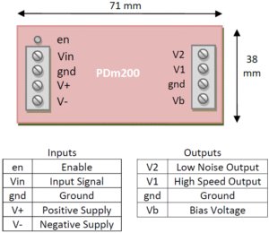
The PDm200 is a high-performance power supply and linear amplifier module for driving piezoelectric actuators and other loads. The output voltage range can be switched between bipolar or unipolar modes with a range of 100V, 150V, or 200V. In the unipolar mode, the negative output range is fixed at -30V for use with stack actuators. The PDm200 can drive stack actuators; standard piezoelectric actuators; two wire benders; and three-wire piezoelectric benders requiring a bias voltage. The PDm200 is suited to a wide range of applications including: Electro-optics, ultrasound, vibration control, nanopositioning systems, and piezoelectric motors. There is short-term protection for over-current and temperature. The module can be mounted to a base with four M2.5 screws. The PCB mounting version is supplied with headers for direct mounting onto a host motherboard. Download Datasheet EU Declaration of Conformity Compatible Actuators Stack Actuators 60V, 100V, 120V, 150V, 200V Plates and Tubes Up to +/-200V Two Wire Benders Up to +/-200V Three Wire Benders 0 to 200V with 200V bias Specifications Power Supply+/-12 V to +34 V Max Unipolar Output-30V to 200 V Max Bipolar Output+/-200 V Peak Output Current 300 mA RMS Output Current 120 mA (+/-100 V Output) Power Bandwidth 63 kHz (100 Vp-p) Signal Bandwidth 200 kHz Slew Rate 20 V/us Dimensions 71 x 38mm Weight 50 g Gain 20 V/V Input Impedance 200 kOhm Input Offset+/-10 mV Load Any Overload Protection Short-term over-current and temperature Noise 1 mV RMS (1uF Load) Environment 0 to 60C (32 to 140F) Quiescent Current 100 mA (7.5mA in Shutdown) Connections Connection Diagram Operation A power converter generates a unipolar or bipolar supply. The output voltage range is controlled by the voltage selector jumpers. The amplifier has a gain of 20 and an input voltage range of +/-10 V. The load is connected directly to the high-speed output (V1) or through a filter (V2) which reduces the noise and bandwidth. In most applications, the V2 output is recommended. A variable bias supply is also available for piezoelectric bender applications. The default bias voltage is 200 V but lower voltages can be achieved by adding a resistor. Block Diagram Example Applications Application Circuits Configuration The PDm200 is configurable to suit a wide range of power supply and output voltage ranges. The output voltage range is selected by two jumpers marked L1 and L2, as shown below. Each jumper has four possible positions marked by the letters A to D and E to H. Voltage Configuration Jumper Locations In the unipolar output mode, the negative output range is fixed at -30 V and the jumper L2 is always in the 'E' position. The correct position for the L1 jumper is listed below for different power supply voltages. Output Voltage Power Supply Voltage Max Min +/-12V to +/-14V +/-15V to +/-17V +24V to 30V +30V to 34V 200V -30V D D 150V -30V D C D C 120V -30V C B C B 100V -30V B A B A Unipolar Jumper Configuration With a single supply, the negative output voltage range is reduced from -30 V to -20 V. In bipolar output mode, the correct positions for the L1 and L2 jumpers are listed in below. In the +/-200 V mode, the low-noise output (V2) is recommended. See "Stability" for more details. Output Voltage Power Supply Voltage Max Min +/-12V to +/-14V +/-15V to +/-17V +24V to 30V +30V to 34V 200V -200V D,H D,H 150V -150V D,H C,G D,H C,G 100V -100V B,F A,F B,F A,F Bipolar Jumper Configuration The PDm200 can also be used in lower voltage applications; however, the output current may be reduced. The corresponding low-voltage jumper positions are listed below Output Voltage Power Supply Voltage Max Min +/-12V to +/-14V +12V to +15V 80V -30V A,E 80V 0V D,E 60V -60V D,H Low Voltage Jumper Configuration Output Current The peak output current is approximately 300 mA and the maximum average DC output current is approximately where is the differential supply voltage e.g. 30V, and is the differential output voltage range e.g. 400V. The average DC current is the average current flowing in either the positive or negative direction. For a sine wave, the average DC current is related to the RMS current by The PDm200 calculator can be used to estimate the maximum input and output current for a given supply voltage and output voltage range. Some common values are tabulated below. Output Voltage RMS Current Average Current Max Min 150V -30V 144 mA 65 mA 200V -30V 108 mA 49 mA 100V -100V 128 mA 58 mA 200V -200V 53 mA 24 mA RMS and Average Output Current for a +/-15 V Supply Supply Current The maximum supply current is 0.5 A at full load. For a partial load, the supply current is where the required input power is where is the differential output voltage range and is the average output current. Power Bandwidth The calculator below plots the maixmum peak-to-peak output voltage for a capacitive load versus the frequency and voltage range. With a capacitive load, the power bandwidth is limited by the average output current. The maximum frequency sine wave is The power bandwidth is primarily related to the average current limit as described above. However, when operating at full range, e.g. +/-200 V, with the minimum supply voltage, e.g. +/-15 V, the power supply droop can distort the top of a signal. This effect can be reduced by increasing the supply voltage. Signal Bandwidth With a load capacitance greater than 100 nF, the small signal bandwidth is With a load capacitance less than 100 nF, the small signal bandwidth is approximately 200 kHz. The bandwidth of the low noise output (V2) is approximately 5% of the high speed output, that is, The small signal bandwidth for a range of capacitive loads is listed in the table below. Load Capacitance High Speed Bandwidth Low Noise Bandwidth 10 nF 200 kHz 49 kHz 30 nF 200 kHz 20 kHz 100 nF 158 kHz 6.6 kHz 300 nF 52 kHz 2.3 kHz 1 uF 15 kHz 690 kHz 3 uF 5.2 kHz 230 kHz 10 uF 1.5 kHz 69 Hz 30 uF 530 Hz 23 Hz Small signal bandwidth Noise The output of the PDm200 contains a small amount of switching noise from the boost converter and random noise from the high-voltage amplifier. With a +/-15 V supply and +/-100 V output range, the RMS noise is listed below. Load Capacitance High Speed Output Low Noise Output 10 nF 4.1 mV 1 mV 100 nF 1.3 mV 0.3 mV 1 uF 1.3 mV 0.2 mV 10 uF 0.42 mV 0.1 mV RMS Noise versus load capacitance For applications requiring low noise, a larger resistance can be used to reduce the effective bandwidth, which is approximately where is the load capacitance. The recommended bandwidth in low-noise applications is 100 Hz. The noise measurements were performed with the input shorted. The noise may increase when significant current is drawn from the output due to ripple from the boost converter. For load capacitances of 100nF or smaller, the low noise output (V2) is recommended. The noise from the PDm200 internal switching power supply includes a common-mode noise current that flows into the module ground. This can appear as fast voltage 'spikes' that occur at intervals of approximately 2.5us on the input and output signals, and the power supply connections. Common-mode noise is exacerbated by ground loops and wiring inductance. To reduce the common-mode noise, the following techniques can help: - Use a twisted pair (for single supplies) or a braided triple (for dual supplies) to connect the module to the power supply. Minimize inductance by using a tight braid or twist. - Use a separate twisted pair to connect the input signals, and the load. - For further reduction, wind 5 to 10 turns of the twisted pair or braid around an ungapped ferrite toroid, e.g. a 1-inch Fair-Rite 5975001401. There should be a 1mm gap between adjacent turns, do not let the turns contact each other. It should be noted that the common-mode noise is approximately equal on the output signal and ground; therefore, if there is no separate connection to an external ground at the load, the common-mode noise will not result in a significant voltage difference at the load. Standard oscilloscope probes are grounded and will exaggerate the effect of common-mode noise. To measure the true output noise at the piezo, a differential or isolated probe is required. If this is not available, a high-frequency isolation transformer in series with an AC decoupling capacitor is possible. Application Notes The amplifier input should not be left floating as it will drift towards a supply rail. However, in applications where the input may float, a 1 kOhm resistor (1206 size) can be mounted at the location "Rin", the input impedance is now 1 kOhm. Heat Dissipation At full power, the worst-case heat dissipation is approximately 15 W which is dissipated by the heatsink and fan. During normal operation the heat dissipation can be estimated by multiplying the required supply current and the differential supply voltage. When the heat dissipation is less than 5W, the module fan can be removed. A high-performance passive heatsink is also available (PDm200-Fanless). Note that the power dissipation in the +/-200V output range is always greater then 5 W so forced air cooling is a requirement. With the passive cooling option, the thermal impedance of the PDm200 from junction to ambient is approximately 10 C/W. An air-flow of 100 LFM or greater is required when more than 5 W is dissipated continuously. The PDm200 will shut down when the heat-sink reaches 70 C. Stability In the +/-200 V range, oscillation can occur with some load capacitances when the output voltage is very close to the negative rail (-190V). This problem can be eliminated by using the low-noise output (V2). Alternatively, a 330pF 25V 0603 capacitor can be soldered on top of R14 which reduces the bandwidth to approximately 3 kHz and will avoid oscillation. This capacitor can be installed before delivery if necessary. Bias Output The bias output (Vb) provides a fixed +200 V output for driving 200 V three-wire actuators like benders that require a bias voltage. Actuators that require a +/-100 V bias can also be driven in this configuration as this is electrically identical. Lower bias voltages can also be achieved by adding a 1206 resistor to the location "Rb". The resulting bias voltage is For example, if Rb is 2.7 MOhm, Vb = 148 V. The bias output can sink or source an average current of 10 mA. However, there is no protection so care must be taken not to exceed the current limit. If more than 10 mA is required, the primary output of a second PDm200 can be used to generate the bias. 200V Three wire bender driver with bias Enable / Shutdown When the amplifier is Enabled and operating, the green LED is on. If the LED off, or flashing, the causes and associated test procedures are: - The output current has been exceeded. Try reducing the frequency or voltage, or disconnect the load to test the module; - The temperature limit has been exceeded. Check that sufficient air-flow is available, the fan is spinning, and the heatsink is not fouled with dust; or - The supply voltage is not sufficient. Check the supply voltage. If the current rating is too small, some power supplies will continually cycle. The Enable pin is a high impedance signal that floats 5V above the negative supply rail. It can be pulled to the negative supply rail to disable the amplifier. The voltage on this pin can also be monitored to check the status of the amplifier. Any monitoring circuit should have an input impedance of greater than 200 kOhm. A high level voltage on the enable pin indicates a normal status while a low level indicates a thermal shutdown. The recommended enable circuits for unipolar and bipolar supplies are shown below. Any small signal transistors are suitable, e.g. BC817 and BC807. Enable circuit for unipolar supply Enable circuit for bipolar supply Overload Protection The PDm200 is protected against short-term over-current and temperature. This protection will reduce the risk of damage from single overload events; however, the user is responsible for ensuring that the operating specifications are not continuously or repeatedly exceeded After an over-current event, the amplifier is disabled for approximately 2 seconds, then re-enabled. If the overload condition persists, the amplifier will continue to cycle between enabled and disabled, which will reduce the lifetime and eventually cause failure. If the PCB temperature exceeds 70C the amplifier will be disabled until the temperature reduces. Continuous thermal cycling will reduce the lifetime and will eventually cause failure. Warranty PDm200 modules are tested prior to delivery. There is no warranty period. Continually exceeding the operating specifications, e.g. by repeatedly exceeding the current or temperature limit, will destroy the module. Please refer to Overload Protection. The PDm200 modules are not considered repairable. Support For support, please submit a contact enquiry. High Voltage Safety Warning This product produces potentially lethal voltages up to 220 Vdc. Observe Low-Voltage (as per ANSI C84.1-1989) safety precautions, e.g. - Use an observer trained in low-voltage rescue - Do not operate with exposed conductors - Use appropriate signage Dimensions The mounting posts accept an M2.5 screw. For the PCB mounting version (PDm200-PCB), an Altium schematic and footprint library is available for download. The PCB pin part numbers are Phoenix Contact PST 1.0/5-3.5 and PST 1.0/4-3.5 which are 1 mm diameter, the recommended PCB hole is 1.5 mm. PCB mounting modules can be soldered directly to a board, or mounted with pin receptacles such as Harwin H3161-05. Click here to download 3D model PDm200 V9 Dimensions (mm)
CATEGORY
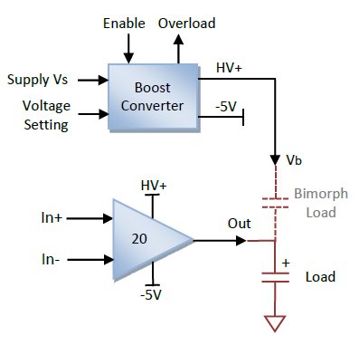
The MX200 is a complete power supply and high-performance linear amplifier module for driving piezoelectric actuators. The MX200 can drive stack actuators; standard piezoelectric actuators; two wire benders; and three-wire piezoelectric benders requiring a bias voltage. Output currents of up to 1 Amp are developed at frequencies up to 100 kHz. Bipolar output voltages up to +/-100V are possible with an external AC coupling capacitor. The MX200 is protected against short-circuit, average current overload, and supply under-voltage. The MX200 can be used as a stand-alone module or mounted to a base with four M3 screws. The PCB mounting version (MX200-PCB) is supplied with headers for direct mounting onto a host motherboard. Compatible Actuators Stack Actuators 60V, 100V, 120V, 150V, 200V Plates and Tubes up to +/-200V Two Wire Benders 0 to 200V with 200V bias Three Wire Benders +/-100V with +/-100V bias Specifications Power Supply 24 V (18 V to 36 V) Voltage Range +100 V, +150 V, +200 V RMS Current 550mA, 330 mA, 220 mA Peak Current 1 Amp Power Bandwidth 106 kHz (180 Vp-p) Signal Bandwidth 200 kHz (100 nF Load) Slew Rate 60 V/us Gain 20 V/V Input Impedance 33 kOhm (In+), 1.6 kOhm (In-) Input Offset +/- 5 mV Load Unlimited Output Noise <1 mV RMS (1uF Load) Protection Over-current and under-voltage Quiescent Current 0.3 A (30 mA in shutdown) Dimensions 80 x 46 x 40 mm (L x W x H) Environment 0C to 60C (-40F to 140F) Weight 95 gram Operation A boost converter generates the high voltage supply and negative rail. The output voltage range can be set to either +100V, +150V, or +200V. Configuration options are discussed in the following section. Bipolar output voltages up to +/-100V are possible with an external AC coupling capacitor, refer to "Bipolar Output Voltage". The high-voltage amplifier has differential inputs with a gain of 20 and an input voltage range of 10 V. The negative input can be connected to ground or to a differential source. It should not be left floating. The load is connected between the output and ground. The bias voltage output is for three wire bimorph bender actuators. Configuration The output voltage range can be set to either +100V, +150V or +200V using the two jumpers LK1 and LK2. Greater output current is available in the lower voltage ranges. Incorrect jumper combinations will damage the amplifier. Voltage Range Peak Current RMS Current Average Current LK1 LK2 100 V 1 Amp 550 mA 250 mA A Out 150 V 1 Amp 330 mA 150 mA B B 200 V 1 Amp 220 mA 100 mA Out A Output Current The maximum continuous RMS current is dependent on the voltage range, as described in Table 1. The average positive output current is also useful for calculating power dissipation and the average supply current. For a sine wave, the average positive output current is equal to The peak current limit for all voltage ranges is +/-1A, which can be supplied for up to 5ms. This is useful in pulse applications where a fast rise-time is required. Supply Current The quiescent power for the amplifier and fan is approximately 8 W. Therefore, the quiescent supply current at 24 V is 0.3 A. This can be reduced to 30 mA by applying a logic zero to the Enable pin. The supply current is related to the average positive output current by where is the output voltage range, and is the average output current. Therefore, the maximum supply current is 1.25 A with a 24 V supply at the full rated power (=100 mA). The power supply must be sufficient for the amplifier, a rating of at least 1.5 Amps is recommended. Note that when power is first applied or when the amplifier is enabled, full current will be required for a brief period to charge the storage capacitors. Bias Output for Piezo Bimorphs The bias output (Vb) provides a fixed voltage for driving three-wire piezoelectric benders. The bias voltage is approximately 5V above the selected voltage range. The effective capacitance when using bimorph actuators is the sum of both layers. Actuators that require a symmetrical bias voltage, e.g. +/-100 V can also be driven since this configuration is electrically identical to the unipolar configuration, e.g. 0V to 200V. Power Bandwidth The calculator below plots the maixmum peak-to-peak output voltage for a capacitive load versus the frequency and voltage range. The maximum frequency with no load is limited by the slew-rate of 60 V/us. That is, With a capacitive load, the power bandwidth is limited by the output current. The maximum frequency sine wave is where is the average current limit (100 mA for the 200V range), is the peak-to-peak output voltage, and is the effective load capacitance. Small Signal Bandwidth Load Capacitance Bandwidth 10 nF 180 kHz 30 nF 283 kHz 100 nF 275 kHz 300 nF 160 kHz 1 uF 78 kHz 3 uF 30 kHz 10 uF 8.3 kHz 30 uF 3.0 kHz Noise The output noise contains a low frequency component (0.03 Hz to 10 Hz) that is independent of the load capacitance; and a high frequency component (10 Hz to 1 MHz) that is inversely related to the load capacitance. Note that many manufacturers quote only the AC noise measured by a multimeter (20 Hz to 100 kHz) which is usually a gross underestimate. The noise is measured with an SR560 low-noise amplifier (Gain = 1000), oscilloscope, and Agilent 34461A Voltmeter. The low-frequency noise is plotted below. The RMS value is 360 uV with a peak-to-peak voltage of 1.8 mV. The high frequency noise (10 Hz to 1 MHz) is listed in the table below versus load capacitance. The total noise from 0.03 Hz to 1 MHz can be found by square summing the RMS values, that is. Load Cap. HF Noise RMS Total Noise RMS 10 nF 1.5 mV 1.5 mV 30 nF 2.6 mV 2.6 mV 100 nF 3.5 mV 3.5 mV 300 nF 1.2 mV 1.2 mV 1 uF 306 uV 470 uV 3 uF 129 uV 380 uV 10 uF 100 uV 370 uV 30 uF 120 uV 380 uV The majority of high-frequency noise is due to ripple from the boost converter (at 170 kHz). In ultra-low noise applications, the output bandwidth can be restricted to 10 kHz which reduces the noise to less than 100 uV RMS in the 10 Hz to 1 MHz frequency range. This can be achieved with the RLC filter shown below. The required inductance and resistance is where is the cut-off frequency (10 kHz) and is the load capacitance. The inductor should be rated for at least 1 A with a self-resonance frequency of greater than 1 MHz. A first-order resistive filter can also be effective, although it must be rated for the expected RMS current. The required value is Optimal Noise Performance The MX200 has an internal boost converter which results in approximately 1A current ripple between Pin 7 and Pin 8. To minimize ground noise due to the supply impedance and wiring inductance, use twisted pair wiring. Aluminium Polymer capacitors are recommended between pins 7 and 8 (35V, 1000uF to 10,000uF). The total capacitance should be less than half the maximum capacitance specification of your 24V supply. The MX200 has a differential input to minimize the effect of ground voltage disturbances. The signal source should be connected by a twisted pair cable to Pin 1 and Pin 2, preferably with a grounded shield. For the standard non-inverting configuration, the signal source ground should be connected to Pin 1 at the signal source. If noise is a critical concern, the output filter described above should be considered. When measuring output noise, ensure the probe ground and signal leads are connected directly connected to the load. Do not use remote ground connections. Overload Protection / Shutdown The MX200 is protected against short-circuit and average current overload. The module is also disabled when the input supply voltage is less than 12 V. Current overload conditions are signaled by +5 V on the Overload pin. The amplifier can be shutdown manually by pulling the Enable pin low with an open-collector, or open-drain circuit. The Enable pin normally floats at 6.2V and should not be driven directly. Bridge Configuration The output voltage range can be doubled to +/-200 V by driving the load in a bridged configuration as shown below. In this configuration, the output voltage is That is, a 0V to 10V input produces +/-200V at the load. Zero volts across the load occurs when the input voltage is +5V. However, note that the absolute voltage of each terminal is still +100V. The power bandwidth for this configuration can be calculated by considering only one amplifier and doubling the effective capacitance. Bipolar Output Voltage Bipolar output voltages can be achieved by adding an external AC coupling capacitor, as shown in the diagram below. This approach creates a high-pass filter with a cut-off frequency of 1 Hz. That is, frequencies below 1 Hz will be strongly attenuated. Up to +/-100V can be obtained using the 200V range, or +/-75V using the 150V range, or +/-50V using the 100V range. C1 should be rated for at least the full output voltage of the amplifier. For example, to achieve +/-100V using the 200V configuration, a 250V rated capacitor is required. The capacitance of C1 should be large enough to ensure the series voltage drop is less than 1% of the output voltage. Film capacitors are preferred but electrolytic capacitors are also suitable. If the load is a piezo or capacitor,. If the load is not capacitive at the operating frequency, the impedance of C1 should be less than 1% of the load impedance, that is, The resistor R1 sets the AC coupling frequency, which is recommended to be 1 Hz. The value of R1 is The power rating of R1 should be greater than, where is the RMS voltage across the load. Warranty / Support MX200 modules are comprehensively tested for specifications and overload protection prior to shipping. The user is responsible for ensuring correct setup and operation within specifications. There is no warranty period. Continually exceeding the operating specifications, for example, by repeatedly exceeding the current limit or input voltage rating, or not providing sufficient cooling, will destroy the module, which will need to be replaced at the users cost. MX200 modules are not considered repairable. For support, please submit a contact enquiry to create a support ticket. High Voltage Safety Warning This product produces potentially lethal voltages up to 220 Vdc. Observe Low-Voltage (as per ANSI C84.1-1989) safety precautions, e.g. - Use an observer trained in low-voltage rescue - Do not operate with exposed conductors - Use appropriate signage Dimensions The mounting posts accept M3 screws. For the PCB mounting version (MX200-PCB), an Altium schematic and footprint library is available for download. Click here to download 3D model
CATEGORY
