By NenoVision
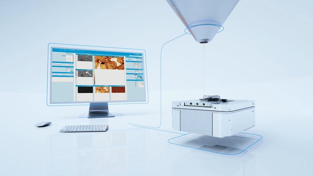
This award-winning tool within the field of In-Situ Correlative Microscopy has the potential to revolutionize the way you perform correlative analysis. - In-situ multimodal & correlative analysis - Optimized & time-efficient workflow - Ultimate performance inside SEM - Open-hardware design for easy customization The new generation of LiteScope AFM-in-SEM is built on the completely new state-of-the-art control unit NenoBox leveraging the performance and capabilities of the AFM-in-SEM to the new level.
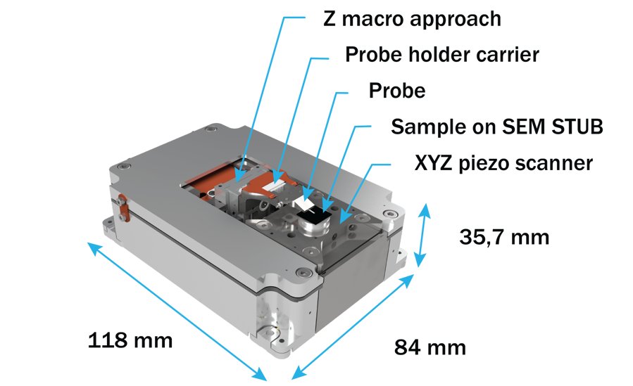
Unique Atomic Force Microscope LiteScope is designed to merge the strengths of AFM and SEM techniques, resulting in effective workflow and extending the possibilities of correlative microscopy and in-situ analysis that ware difficult or almost impossible by conventional instrumentation. - In-situ multimodal & correlative analysis - Optimized & time-efficient workflow - Ultimate performance inside SEM - Open-hardware design for easy customization Novel method of correlative imaging Complex, yet time-efficient analysis via Correlative Probe and Electron Microscopy (CPEM) allows 3D correlative imaging that eliminates the need for repetitive tasks previously required to achieve similar kind of results. All-in-one solution for automated in-situ analysis of multiple material properties enables unique combination of data such as topography, material contrast, mechanical or electrical properties resulting in three dimensional CPEM images. Complex in-situ characterisation AFM brings new inside-to-SEM method of characterisation, enabling the analysis of a broad range of properties: Material mechanical properties topography local elastic properties (tapping & contact mode) local sample hardness (non-topographic) depth-dependent material characterization various in-situ operations Material magnetic properties magnetic domain imaging Material electro-mechanical properties piezoelectric domain imaging Material electrical properties conductivity map (including insulated areas) local surface potential local electrical properties (non-topographic) sub-nanometer topography Installation package: LiteScope – scan head NenoBox – control unit NenoView – control software SEM adaptation plate Vacuum feedthrough Cabling Technical specification Dimensions XYZ 118 mm x 84 mm x 35.7-48.4 mm Scan range in open loop XYZ (±10%)100 μm x 100 μm x 20 μm Total weight 460 g Scan range in closed loop XYZ 80 μm x 80 μm x 16 μm Vacuum working range 10 5 Pa to 10-5 Pa Resolution XYZ up to 0.2 nm × 0.2 nm × 0.04 nm Operating temperature+10 °C to +35 °C Maximum sample height 8 mm Maximal scanned sample area XYZ 21 mm x 11 mm x 8 mm Maximum sample weight 100 g
CATEGORY
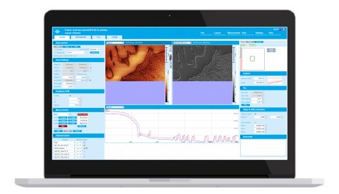
Online-based NenoView software offers a wide range of features that assure time-efficient and easy work with LiteScope AFM-in-SEM: Web-based interface with remote access to user data Intuitive UI adaptable to customer’s needs AI-driven topographic correction Method-based automated probe tuning Single-click operations eliminating repetitive tasks AFM and SEM multichannel data aquisition Schematics of device configuration Possibility of measurement control via inbuilt scripting features Compatible with Gwyddion or MountainsSPIP software for further data postprocessing
CATEGORY
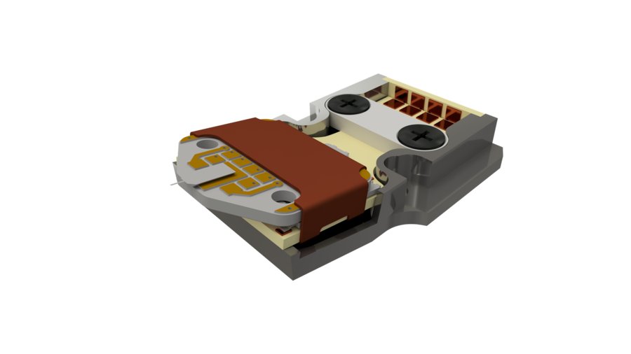
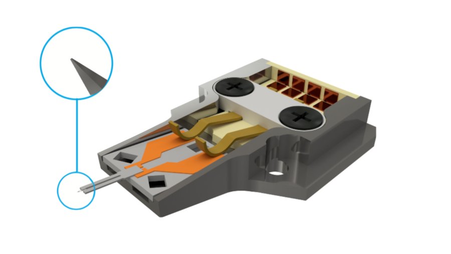
Our new self-produced self-sensing probe with a locally grown platinum tip. Ideal for high-resolution conductivity measurements and characterization of nano-features, expanding the possibilities of the existing NenoProbe Conductive. Fully compatible with our current NenoProbe holder. Measurement modes: C-AFM, Topography, I-V spectroscopy
CATEGORY