By IntelliSense
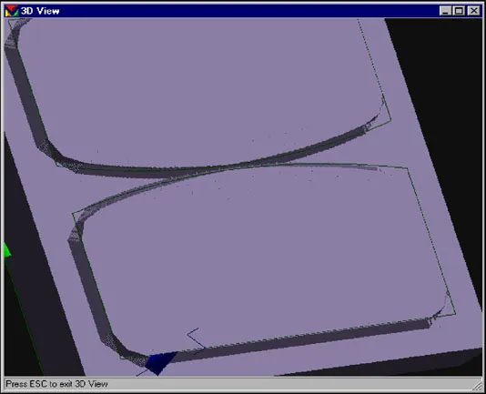
AnisE is an easy-to-use anisotropic etch process simulation tool for MEMS design and process control Demystifying etch behavior Anisotropic etching is one of the most difficult silicon micro-machining processes to model, often considered in the realm of the black arts. It can be challenging to grasp intuitively due to the complex nature of evolving etch fronts. In fact, many companies have developed closely guarded etch secrets through trial-and-error experimentation. Well, those days have ended. AnisE simplifies the process of accurately simulating etch behavior. Import your mask, choose your wafer orientation and your process parameters, and then watch the etching progress online before your eyes! Cellular automata Unlike other tools that utilize heuristic methods to calculate propagation of etch planes, AnisE is a cellular automata based simulation. What does this mean? That other tools fail to provide accurate results for complex masks and long etch times. With AnisE, you can choose any mask configuration, however complex, throw in double-sided etching and add etch stops. Its easy AnisE at work 3D evolution of Silicon etch profiles generated by AnisE are shown in three cases. (a) evolution of three different corner compensation schemes (b) double-sided etching of a silicon boss for an accelerometer application and (c) multi-etch of silicon, an example where DRIE is followed by an anisotropic etch. Sophisticated controls AnisE comes with built-in etch databases for KOH and TMAH. It automatically updates the etch rates as a function of temperature and concentration. With AnisE, you can simulate single or double-sided <100> and <110> etching. You can incorporate multiple etch stops, steps or anything else you can do in the real world. In addition, you can study the effect of mask misalignment, the effect of combining RIE etching with anisotropic etching and many other real- world conditions. Whether you are interested in studying process variation or designing corner compensation features, AnisE will become an invaluable part of your process toolset. Comprehensive Capabilities AnisE is capable of predicting the effects of etchant temperature, concentration, and etch time on the final 3D device geometry. Corner compensation and process tolerances can be modeled and visualized with AnisE. Creating correct geometries based on proper etch parameters before entering a fabrication facility saves resources otherwise spent on multiple prototype iterations. Top features By creating or importing a mask file, users can: - Simulate <100> or <110> wafer orientation etching - Simulate etching under different time, temperature, and concentration parameters - Access TMAH and KOH etch-rate databases, or use customized etch-rate data - Etch the top, bottom, or both sides of a wafer - Implement multiple protective etch stops - Perform multiple etchings with different masks on a single wafer - Study the effects of misalignments and other process deviations - Determine the effects of vertical etching coupled with anisotropic etching - Perform 3D geometric visualization and cross-sectioning - Take distance measurements on the etched wafer - Visualize and export 3D results in DXF and VRML formats
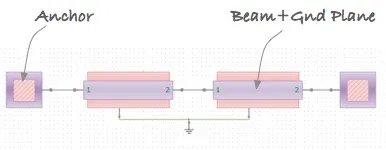
Developed by IntelliSense to answer the unique needs of the microsystem and nanosystem community, SYNPLE is a system-level simulator for multiscale (macro, micro, nano) phenomenon simulations. As a MEMS design professional, you always seek new ways to realize your designs and, ultimately, bring them to market. With SYNPLE, you can. This revolutionary tool will enable you to work in multiple domains - simply and without limits. Do your current simulation tools stifle the reach of your imagination? Impose limitations on your designs and work product? SYNPLE will allow you to follow your out-of-the-box vision - and create simulations to match. SYNPLEs advanced element libraries, user-defined elements and a user-expandable architecture will significantly increase your present multi-physical simulation capabilities. As a result, you can explore a whole new design universe and be as creative as you want to be! When IntelliSense developed the SYNPLE system-level simulator, we incorporated user benefits that would make a real difference to your bottom line, rather than adding lots of extraneous bells and whistles. First and foremost, SYNPLE enables you to explore a large design space in a short amount of time - which maximizes your time and creativity. To save time further, it allows you to funnel, and quickly whittle down, a large number of design options. And to minimize your manufacturing costs, SYNPLE makes it possible to understand the ultimate impact of your design parameters on manufacturing yield. Enjoy maximum creativity at minimum time and cost - it's that SYNPLE! While SYNPLE's range is wide enough to create complex simulations, its user interface is exactly what the name implies - simple! In fact, if you've ever created a flow chart (who hasn't in this business?), then you'll take to SYNPLE like a fish to water. By relying extensively on the familiar "drag-and-drop" function, rather than arcane interfaces, its both easy to learn and easy to use. Automatic bus-based wiring: SYNPLE's new auto-wiring feature eliminates the need to manually connect all of your elements. Thermal, electrical, mechanical, piezoresistive, and electronic properties are all connected through one bus-based wire. Not only does this make the schematic much easier to read, it eliminates the tedious task of drawing multiple wires, allowing you to focus on what's really important - designing! SYNPLE's auto-wiring feature makes it easy to build up a complex device in minutes. Thermal, electrostatic, mechanical, piezo, and electronic properties are all connected through one bus-based wire. Friendly manager windows make it easy to define your ambient fluid parameters, material properties, and element parameters. Just input the data once, and it will be automatically saved and inserted into the relevant calculations. Elements, unlimited: To further your capabilities, IntelliSense ships SYNPLE with an extensive line of comprehensive element libraries for your use. These include analog, digital, mixed-signal, micromechanics, semiconductor, MEMS and biological libraries. You can even use advanced elements such as multi-layer, CMOS, or piezoelectric beams. Whether it be radial comb drives or common MEMS spring designs, we have taken into account everything that a MEMS designer would need. Develop from the top, down: SYNPLEs top down modeling capability enables you to drag and drop individual elements from different domains and wire them up to create complex systems. For instance, you might use elements from SYNPLEs MEMS library - which includes atomic elements like beams and plates, compound elements like serpentine springs and comb drives, and device elements like switches, accelerometers and gyros - to create your own complex systems from the bottom up. Build from the bottom, up: Is bottom-down modeling a more desirable capability for your needs? If so, then SYNPLE makes that simple as well - allowing you to import your existing finite element models and combine them into new, more complex systems. 3D Macro-modeling in Synple: IntelliSense extracted system models are full 3D models. Hence, Synple can provide full 3D output of the system response. As a result the response of a device to a complex mechanical or electrical input can be captured accurately. (a) Extracted beam model responding to a 50 kHz voltage input, note the initial deformation in the beam shape due to residual stress effects (b) the same beam responding to a 3 MHz voltage input (c) a micro-mirror response showing multiple modes being actuated. The seamless integration of System Model Extractor (SME) with SYNPLE is a powerful combination that allows you to create accurate N-DOF (n degrees of freedom) device-level black box models that fully capture the dynamic and harmonic responses of even the most complex of MEMS devices. Our tests have shown a 100-1000x improvement in speed in performing dynamic analyses compared with traditional FEA. Powerful data analysis: SYNPLE links to the new WaveRunner waveform and data analysis tool. With WaveRunner, you can easily create and export professional-looking plots. WaveRunner comes with a number of plot templates ranging from simple charts to Bode plots to sophisticated trajectory plots and parametric exploration 3D plots so that you can explore your data with ease. Multiple cursors (x and y) are available to measure distances along any dimension. Whether you're creating a multi-curve or Monte Carlo plot (or any plot in between), you won't find a result analysis tool that is more powerful or easier to use. Multitude of plot templates: WaveRunner capabilities extend from simple waveform analysis to sophisticated data analysis. Users can create and explore data in a number of publication ready formats. Schematic based 3D System modeling: Graphs and charts are great, but haven't you ever wished you could really see what the behavior of your system looks like? Now you can! SYNPLE can directly export the results of your simulation to the 3D post-processing module VisualEase. In VisualEase, you can view full 3D animations of your system simulations. Fast 3D results: SYNPLE allows you to visualize your system response in 3D without having to go through tedious FEA modeling. 3d results can be obtained in seconds. 3D animations of classic MEMS systems are shown above. This includes, a Bandpass filter, a mode matched tuning fork gyro and the classic Tang Resonator.
CATEGORY
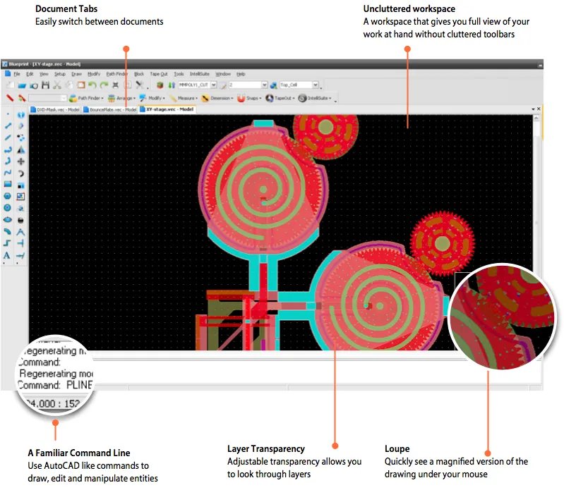
Tired of using IC layout tools for MEMS? We certainly were. When you think about it, MEMS layout is one of the most cumbersome parts of the design process, involving countless revisions, incompatible data formats and minute details. The challenges of MEMS layout are compounded further by the fact that most tools available are IC layout tools, or less-appropriately, architectural design tools. Finally, a layout tool for MEMS Blueprint is the first layout tool designed specifically for the MEMS community. Our goal with Blueprint was to revisit the workflow of the layout engineer and create a tool that would be effortless to learn and use. Our design philosophy for Blueprint is: "simple things should be simple, complex things should be possible." That's why our product provides configurable palettes that you can drag and customize to your needs; clearly illustrated icons; and configurable grids and guides - all of which make device layout easier than ever. We even went a few steps further... automatically linking masks created in Blueprint to process steps for creating 3D visualization of your device. What's more, Blueprint users can now link the layout with automatic mesh creation and refinement for device-level analysis! Zen and the art of MEMS custom layout Full custom layout requires your undivided attention on the job at hand. That is why we designed Blueprint with a minimalist sensitivity that maximizes the drawing area. Cells, layers, grids are all available at your fingertips, but take up very little real estate, panels neatly hide after you have used them, toolbars can be torn-off and repositioned to you liking and then closed when you don't need them. All-in-all, providing a very zen experience so that you can draw and edit away without distractions! Stop playing the parking valet Current layout tools treat you like a parking attendant at a crowded lot. Constantly shuffling between views and managing a lot of administrative trivia like layer visibilities, grid sizes, snaps, cells and views. Blueprint introduces a simple solution - Bookmarks. A Bookmark can contain layer states, grid preferences, viewports, view states, grid information, snap settings, transparency settings, and cell states. Add a bookmark and your current settings are saved. You can then switch to other parts of the drawing. Switch back to a bookmark, and you are back to the drawing, exactly as you left it before. Command line and keyboard shortcuts If you've ever used AutoCAD, then Blueprint will seem very familiar to you. Run commands from the command line or use the customizable keyboard shortcuts for quick and easy drawing. Enjoy a familiar interface coupled with the immense capability of a layout editor specialized for MEMS design. Customizable interface Blueprint makes it easy for you to tailor the interface to your liking. Customize keyboard shortcuts and manipulate toolbars and snap settings to match your drawing style. Modify performance parameters to adjust redraw speed and level of visible detail. When you're finished, save the information to a user profile, so you can easily load your customized settings later. Drawing tools for MEMS designers No other layout tool is so optimized for MEMS design as Blueprint. Advanced drawing tools like Béziers, splines, and poly-lines are a breeze to use, and multilingual text is fully supported. Use the Pathfinder operations (add, intersect, subtract, divide, NOR, XOR, grow, shrink, make ring, extract ground plane) to quickly create complex shapes. Modify, align, or distribute shapes easily using the keyboard or the mouse. Easy snapping The possibilities are endless when it comes to Blueprints snap settings. Snap to common features like endpoint, midpoint, center-point, or intersection points or more advanced features such as tangential or perpendicular points. You can even snap to polar angles and distances in the absolute frame or relative to other objects. The toolbar is fully customizable, so you can select any combination of snaps to be active at a given time. Measurement and dimensioning tools With Blueprints measurement functions, you can easily measure linear distances, perimeters around a specific shape, or areas of selected objects. Easily add dimensions to your drawing and customize them to the style of your choice. Full cell hierarchy support If you're working with cells and arrays, then Blueprint is the tool for you. Blueprints Cell Manager makes it easy to keep track of cells and manage their hierarchy. You can easily edit and insert cells and arrays and scale or rotate them to your liking. Cross-section viewer Ever had troubled visualizing what your mask looks like in 3D? Blueprint solves that problem! Just select a process flow to reference, draw a line across any part of your mask, and instantly see the cross-section of the device along that line. Not only can you see the final cross-section, but you can jump to any step of the process flow to see the cross-section at that step. PowerPoint export Anyone who has ever tried to hand-draw a process flow in PowerPoint knows how time-consuming it can be. Thankfully, Blueprint can create one for you with the click of a button. The PowerPoint file contains the cross-section and process parameters of every process step, as well as handy summary slides for easy reference. Sharing process information across your organization has never been easier. 3D model visualization 2D cross-sections are great, but sometimes you might want to see your full model in 3D. Blueprint makes this easy with automatic export to FabViewer, the process visualization tool in IntelliSuite. Here you can fully inspect your 3D model and export PowerPoint, image, or video files. Blueprint is fully scriptable, enabling you to create complex parametric cells and drawings through scripting. Blueprint allows full support for Windows Script Host (WSH) which allows language independence for scripting. You can use built in VBScript based scripting or use any language of your choice (Jscript, Python, Perl, Tcl/Tk) by installing the appropriate language support. Or, choose from our large library of scripts that can be modified to suit your needs.
CATEGORY
IntelliFAB allows you to debug your process flow and your mask set even before you enter the clean room. It allows you to make virtual prototypes to save costly fabrication mistakes. Welcome to your virtual fab Until now, MEMS designers have typically focused purely on geometric representation of the device in order to analyze device behavior. The drawback of this methodology is that process induced effects may vary the geometry of the structure significantly. For example, the boron diffusion as an etching stop layer for bulk silicon processing may overstress the structure, strain gradients in poly-silicon structures can distort features, or an anodic bonding process may break down protective oxide films. IntelliFAB allows designers to takes a different approach. Process flow forms the basis of creating your devices. Our comprehensive process simulation modules incorporate deposition, etching, bonding, doping, electroplating, liftoff, and other process steps common in MEMS design. Other process-induced effects, such as micro-assembly, are also addressed to generate accurate geometric models for the complete range of MEMS devices. IntelliFAB is directly linked with MEMaterial, a MEMS process database that stores material properties as a function of your machine settings. By developing the fabrication process in conjunction with the analysis model, IntelliSuite enables engineers to perform more accurate device physics analysis and produce manufacturable devices faster. MEMS Process Editor A typical MEMS process flow can consist of hundreds of process steps which need to be cataloged and debugged; IntelliFAB makes editing and organizing large process tables easy. Built in grouping, filtering, and arrangement tools allow you to section, organize and debug large process tables. IntelliFAB allows you to quickly build and debug your process traveler down to the last detail. Foundry ready templates Processes can be custom-designed one step at a time, or engineers can draw from a wide range of foundry-ready process templates. Users create their own process flows from a database of over 70 process steps or by including custom process steps. Process flows can be saved as templates for repeated use. Support for popular processes MUMPS, SUMMiT-V, Infotonics (SOI Hybrid), AMIMOSIS, Bosch Surface Micromachining, LIGA, Cornell SCREAM is included out of the box Take the pain out of meshing Hexpresso, our mesh synthesis tool is now integrated with IntelliFAB. With click of a button you can create high fidelity, all-hexahedral meshes from the process flow. MEMS Designers can spend up to 70% of their design person-hours creating and manipulating meshes. Solid models created by IntelliFAB can be directly exported to analysis engines with the click of a button, saving you considerable effort and time. IntelliFAB uses true process information along with your mask layouts to create the device model for analysis. Movies Dynamic Cross Sections: View FABViewer Cross-sectioning capability in real-time. Visualize Complex Processes: Virtual prototyping of a mechanism using the Summit-V process Process Debug In Action: See how FABViewer can help you in process debug Slides View Slideshow: IntelliFAB Slideshow(Slideshare) Download PDFs: IntelliFAB Presentation PDF Wrap it up! As a packaging engineer, IntelliSense offers you tools for thermal, mechanical and high-frequency modeling of your devices. Parametric scripting capabilities allow you to effortlessly create a range of packages, such as SOICs, DIPs, QFPs etc. What's more, wafer-level encapsulation and related stress analyses may be performed with ease. As a result, you can wrap up your projects quickly and efficiently! Ace the test Working together, IntelliSuite and SYNPLE give test engineers a straightforward method for creating parametric test structures and design of experiments (DoE) during the layout process. What's more, our analysis and system simulation tools allow you to perform a vast subset of MIL-STD (750/883), JEDEC (JESD22) and Telcordia (Belcore) tests in software before the actual fabrication. For success in your next test, turn to IntelliSuite!
CATEGORY

Use RECIPE to fine tune your RIE, ICP, DRIE, Bosch Etch processes. Predict sidewall profiles and etch issues before you enter the fab. RECIPE for success RECIPE is a powerful, easy-to-use RIE/ICP (Reactive Ion Etch/Inductive Coupled Plasma) etch process simulation tool for use in designing microstructures. With RECIPE, you can layout your microstructure and automatically simulate isotropic, RIE, ICP/Bosch/DRIE etching or any combination of the three processes. RECIPE supports the simulation of both ion-assisted etching and deposition processes. In fact, it is the only tool on the market for simulating the deep etching of silicon and other substrates. Easy Setup IntelliSense recognizes that differences in etch systems can cause a large variance between any simulation and experimental results. In order to minimize these differences, simple setup methodology is provided to calibrate RECIPE models with your etch machines. Bowl and stem etch Simulation of a classic bowl and stem etch showing the evolution of the etching profile. Features such as RIE lag, scalloping, feature size dependency can be seen in the simulation. Sequential Multiple Etches RECIPE allows you to explore novel structures and allows you to tailor your cross-sections on a PC, rather than performing cumbersome and costly clean room experimentation. For instance, you can easily perform an anisotropic RIE etch, an isotropic etch and a Bosch etch — one right after another! In addition, you can use an isotropic etch to explore front-side release of structures. Experimental Validation Click on the above pictures of validation of RECIPE against experimental results. IntelliSense owes a large debt to its University Partners in the development and validation of RECIPE, in particular, Peking University, Institute of Microelectronics. Powerful Capabilities RECIPE offers you the ability to simulate a variety of RIE/ICP-related effects. These include: - Predict sidewall scalloping roughness and periodicity - Predict final dimensions and shape of features - Predict sidewall angles - Simulation of RIE lag. You can estimate how much more quickly larger features etch compared with smaller features as a function of process parameters - Positive angle or negative (retrograde) etching - RIE notching and etch termination (pinch-off) behavior - Front-side release processes in SOI based processes - Bowl and stem etches (combination of isotropic and anisotropic etching) to form wine glass shapes for improved step coverage - Release prediction: isotropic release of plates for poly-silicon-based MEMS - Trench refill and trench isolation simulation for high-voltage circuits - Angled etching of substrates Process Debug In Action See how RECIPE and IntelliFAB can help you in process debug Top features - 3D Visualization RECIPE has now been extended to work efficiently in 3D. RECIPE engine can be used within IntelliFAB as well. - Composite processing Simulate effects of multiple etches - Sidewall and etch lag simulation Predict important parameters such as etch lag and sidewall angles - Validated simulator Rigorous etch characterization experiments - Validated database RSM-derived etch database - Quick results Faster than performing a real etch
CATEGORY
