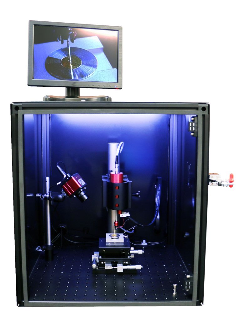
Specification Tip material/diameter: Standard 2 mm gold tip (other sizes and materials available on request) Work function resolution: 1 - 3 meV Probe translation: 25 mm manual translation Visualisation: Single-point work function/contact potential difference measurement Oscilloscope: Digital TFT oscilloscope for real time signal Test sample: Gold and aluminium test sample Control supplied: PC control with dedicated software for fill digital control of all parameters Detection system: Off-null with parasitic capacity rejection Faraday/optical enclosure: 450 mm x 450 mm Optical system: Colour camera with zoom lens and monitor Warranty: 12 Months
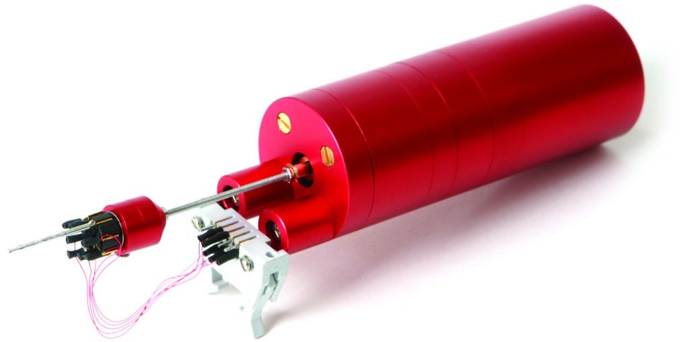
The Kelvin probe is a non-contact, non-destructive vibrating capacitor device used to measure the work function (wf) of conducting materials or surface potential (sp) of semiconductor or insulating surfaces. The wf of a surface is typically defined by the topmost 1 – 3 layers of atoms or molecules, so the Kelvin probe is one of the most sensitive surface analysis techniques available. KP Technology systems offer a very high wf resolution of 1 – 3 meV, currently the highest achieved by any commercial device. The Kelvin probe does not actually touch the surface; rather an electrical contact is made to another part of the sample or sample holder. The probe tip is typically 0.2 – 2.0 mm away from the sample and it measures the ‘traditional work function’, i.e. that found in literature tables. Other techniques, using very sharp tips some 10’s of nanometres away from the sample, measure very reduced and distorted work functions due to the close separation of tip and sample. The physical form of a Kelvin Probe is a head unit containing a voice coil driving system and integral amplifier suspended above a sample. The vibrating tip and the sample forms a capacitor, having ideal, or parallel-plate, geometry. As the tip vibrates electric charge is pushed around the external detection circuit. By careful control of the tip potential and automatic capture and analysis of the resulting waveform both the potential across the capacitor and the capacitor spacing can be calculated to very high resolution. In scanning form the tip is steered across the sample surface using a high resolution 3-axis translator. The spatial resolution of the tip is approximately the tip diameter, we typically use tips of 2.00 mm and 0.05 mm as standard tips in air and anything from a sharp tip to 10.00 mm diameter in ultra-high vacuum. The resulting 3D surface work function images contain information about surface structures, surface composition, thin films, defects, etc. In time-varying mode artefacts such as oxidation (corrosion), defect relaxation, etc can be observed. For semiconductor surfaces, both organic (polymer) and inorganic (Si, Ge, CdS, etc.) the Kelvin probe is the only way to directly measure the Fermi level. Changes in Fermi level, caused by illumination with white or monochromatic light, results in energy band shifts which can be used to characterise interface and bulk defect states. These techniques are termed Surface Photovoltage (SPV) and Surface Photovoltage Spectroscopy (SPS) for which KP Technology can supply both software and accessories for our systems. The traditional Kelvin probe actually produces the work function difference between the tip and sample. The Kelvin method was first postulated by the renowned Scottish scientist Lord Kelvin, in 1861. Typically the tip is first calibrated against a reference surface, such as gold. However KP Technology is the only company to offer absolute Kelvin probes, which combine the Kelvin method and Einstein Photoelectric Effect to produce absolute work function values (in eV). KP Technology has developed dedicated head units for ambient, controlled atmosphere, relative humidity and ultra-high vacuum environments. All of our systems share the off-null, height regulation (ONHR) method invented by Prof. Baikie and consequently produce stable high signal levels resulting in repeatable and high-resolution measurements. The rapid growth of the company since 2000 means the KP Technology systems are found in leading materials research laboratories worldwide. We pride ourselves on our rapid post-sales support and our ability to assist with technical and data interpretation queries.
CATEGORY
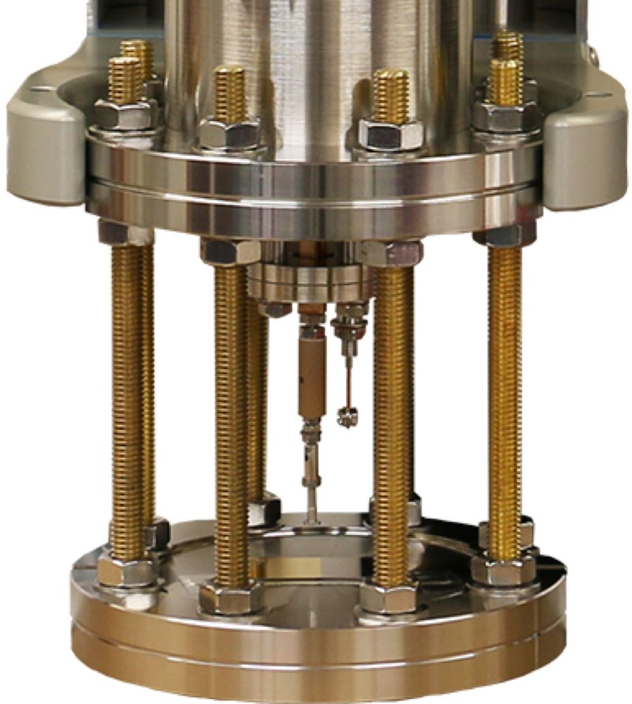
Our Ultra-high Vacuum Scanning Kelvin Probes (UHVSKP2020 and UHVSKP5050) give the user full access to work function (Φ) and contact potential difference (CPD) measurements under vacuum with the ability to scan a sample area of 20 x 20mm or 50 x 50mm respectively. Each system comes with the UHV head unit, tip amplifier (located at the mounting port), digital control unit and host PC with dedicated software. The tip can be retracted 100mm from the sample and approaches normal to the sample. The associated digital electronic unit powers the head unit and provides an interface between the head unit and the data acquisition system. The system comes with a complete user manual, which includes an introduction to work function measurements and a detailed description of the system software, including examples. The work function resolution of the Ultra-High Vacuum Scanning Kelvin Probes is 1-3 meV. The software allows the user digital control of Probe amplitude and frequency, mean-spacing and tip potential. There is also automatic measurement of the Kelvin Probe signal, work function, signal and work function averaging as well as automatic control of tip to sample mean spacing. Other features include variable scan sizes and 3D charting of the work function data. The data generated can be easily exported to Excel-compatible spreadsheets for further processing. Download the product brochure for more information on the Ultra-High Vacuum Scanning Kelvin Probe range, including technical specifications, example measurements and add-on options. - UHVSKP5050 - UHVSKP2020
CATEGORY
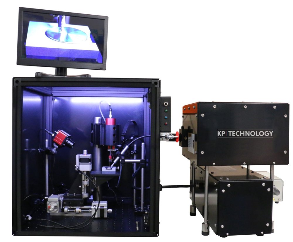
An introduction to our best-selling APS04 system. The Ambient-pressure Photoemission Spectroscopy (APS) system measures the absolute work function of a material by photoemission in ambient conditions, no vacuum is required. The excitation range of APS is 3.4 eV to 7.0 eV, meaning that APS is capable of measuring the absolute work function of metals and the ionisation potential of semiconductors alongside measurement of the surface Fermi level with the Kelvin probe. This system comes with an SPV and SPS source, therefore the full bands of semiconductors can be measured in one complete desktop system; no other product in the world can do this. Specification - Kelvin probe 3-axis scanning - Surface Photovoltage - Surface Photovoltage Specroscopy - Tip material / diameter: 2 mm gold tip - CPD resolution: 1 - 3 meV - Height control (auto): 25 mm automatic - Kelvin probe mode and PE mode: CPD and photoemission measurements - CPD measurement time: CPD measurements in <1 minute - PE resolution: Full photoemission measurement - WF measurement time: PE measurements in <5 minutes - DOS measurements: Full access to DOS information - Optical system: Colour camera with zoom and monitor for positioning - Oscilloscope: Digital TFT oscilloscope for real time signal - Test sample: Gold, aluminium, and silver test samples - Faraday enclosure base (mm): 450 x 450 mm optical and Faraday enclosure - Control supplied: PC control with dedicated software - Patented technology: US:8866505 /GB:2439439 /GB:2495998 /EU:2783205 /JP:6018645
CATEGORY
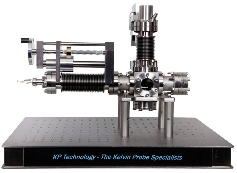
Our Ultra-high Vacuum Kelvin Probes give the user full access to work function and contact potential difference (CPD) measurements under vacuum. Each system comes with a high-quality, manual, or motorized translator that enables reliable and accurate tip-to-sample positioning, and the unrivalled tracking system always holds the tip separation constant during the measurement. Even under vacuum, the work function resolution is 1 - 3 meV. The dedicated software allows full digital control of all parameters to match the exact requirements of the sample under investigation. The recorded data is easily exportable to analysis software. The UHV Kelvin Probe can be mounted to the user's existing UHV chamber or KP Technology offers an elegant UHVKP cell system (UHVKP Corner Cube) that can be used for ambient, UHV or gaseous measurements. This cell is completely modular, and a host of additional extras can be added-on. The latest materials and applications highlighted in published papers includes, solar cells, lead sulfide quantum dots, oxide thin films, silicon terminated diamond, Fischer-Tropsch synthesis and cerium oxide films. Download the product brochure for more information on the Ultra-High Vacuum Single-Point Kelvin Probe range, including technical specifications, example measurements and add-on options. - UHV Corner Cube - UHVKP020-Motorised - UHVKP020-Manual
CATEGORY
