By Graphenea
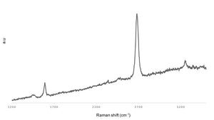
Monolayer Graphene film on Si3N4 (10 mm x 10 mm) - Processed in ISO 7 Cleanroom Monolayer Graphene produced by CVD on copper catalyst and transferred to a Si3N4 substrate using semi-dry transfer process. This product is ideal for R&D departments and universities. Graphene Film - Transparency: > 97 % - Coverage: > 95% - Polymer assisted transfer - Thickness (theoretical): 0.345 nm - Hall Electron Mobility on Si3N4: 1432±428 cm2/Vs - Sheet Resistance: 576±172 Ohms/sq (1cm x1cm) - Grain size: Up to 20 μm Substrate Si3N4 - 150nm of Si3N4 deposited by LPCVD on Si - Type/Dopant: P/Bor - Resistivity: 10-20 ohm.cm - Thickness: 725 +/- 25 μm - Front surface: Single Side Polished - Back Surface: Etched - Particles: <10@0.3 μm Quality control All our samples are subjected to a rigorous QC in order to ensure a high quality and reproducibility of the graphene. - Raman Spectroscopy on each batch: I(G)/I(2D)<1; I(D)/I(G)<0.1 on 90nm SiO2/Si substrate. - Optical Microscopy inspection of each individual sample to ensure good transfer quality and purity If your application requires more specific quality control (AFM, SEM...), please do not hesitate to contact us. Applications Graphene research, Graphene transistors and electronic applications, Graphene optoelectronics, plasmonics and nanophotonics. Graphene photodetectors (measure photon flux or optical power), Biosensors and bioelectronics, Aerospace industry (electronics, thermal interface materials, etc.), MEMS and NEMS Publications “Recent advances in graphene-based biosensors” 2011; doi: 10.1016/j.bios.2011.05.039 “Imaging propagating and localized graphene plasmons by scattering-type SNOM” Nature 2012, vol. 487, 77 – 81; doi:10.1038/nature11254 Downloads Data Sheet Graphene Film download MSDS Graphene Film download
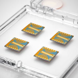
Pack of 4 Pack of 4 1 Unit GFET-S21 (Die size 10 mm x 10 mm)- Processed in ISO 7 Cleanroom The GFET S-21 chip from Graphenea is designed for measurements in liquid medium. The new version provides 12 graphene devices connected in parallel, with encapsulation on the metal pads to avoid degradation and reduce leakage currents; the probe pads are located near the periphery of the chip. It also includes a non-encapsulated electrode at the center of the chip, which allows liquid gating without the need of an external gate electrode (such as Ag/AgCl probes). This device architecture enhances signal-to-noise ratio and reduces parasitics. It also removes device-to-device variation, smoothing device response and improving reliability. Typical Specifications - Growth method: CVD synthesis - Graphene transfer: Polymer assisted transfer - Chip dimensions: 10 mm x 10 mm - Substrate: Si/SiO 2 - Substrate thickness: 675 μm - Resistivity of Si substrate: 1-10 Ω.cm - Gate oxide thickness: 90 nm - Metallization: 50nm Au-based Contacts - Encapsulation: 50 nm Al 2 O 3 - Chip dimensions: 10 mm x 10 mm - Number of GFETs per chip:12 - Optical Yield: ≥75 - Average field-effect mobility (back gating): 1000 cm 2/V.s - Average Dirac point (back gating): <25 V - Average Dirac point (liquid gating): <1 V Absolute maximum ratings - Maximum gate-source voltage (liquid gating in PBS): ± 2V - Maximum gate-source voltage (back gating): ± 50V - Maximum temperature rating: 150 °C - Maximum drain-source current density:10 7 A.cm-2 Quality control All our samples are subjected to a rigorous QC in order to ensure a high quality products. - Optical Microscopy inspection of all the devices - Raman spectroscopy of each fabrication batch - Electrical characterisation (back gating and liquid gating) of each fabrication batch - AFM of each fabrication batch Applications Graphene field-effect transistors (GFETs) have unprecedented sensitivity to the surrounding environment and is an ideal transducer for a variety of sensing applications. Depending on the application, GFETs can be tuned to be sensitive only to the stimulus of interest and have shown breakthrough performance in areas such as graphene device research, chemical sensing, bioelectronics and biosensing. Publications "Graphene Sensor Arrays for Rapid and Accurate Detection of Pancreatic Cancer Exosomes in Patients' Blood Plasma Samples" https://doi.org/10.1021/acsnano.3c01812 "Graphene‑based field‑effect transistors for biosensing: where is the field heading to?" https://doi.org/10.1007/s00216-023-04760-1 "Ultrasensitive detection of SARS-CoV-2 spike protein by graphene field-effect transistors" https://doi.org/10.1039/D2NR05103F "Detection of Glial Fibrillary Acidic Protein in Patient Plasma Using On-Chip Graphene Field-Effect Biosensors, in Comparison with ELISA and Single-Molecule Array" https://doi.org/10.1021/acssensors.1c02232 "Detection of an IL-6 Biomarker Using a GFET Platform Developed with a Facile Organic Solvent-Free Aptamer Immobilization Approach" DOI:10.1109/ACCES.2020.2994611 "High resolution potassium sensing with large area graphene field-effect transistors" https://doi.org/10.1016/j.snb.2019.04.032 Downloads - GFET-S21 Data Sheet download - Measurement Protocols and Basic Handling Instructions download
CATEGORY
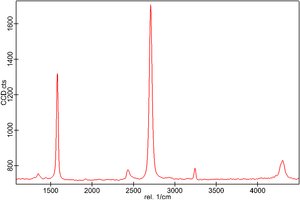
Monolayer Graphene on 90 nm SiO₂/Si - Fully Covered Processed in ISO 7 Cleanroom Our monolayer graphene on SiO₂/Si (fully covered) is a bidimensional material produced by CVD and transferred to a circular substrate of SiO₂/Si (90nm) by a semi-dry transfer process. We consider it to be a benchmark product in the graphene market - not only for its excellent quality, but also for its shape, size and number of applications. Graphene Film - Growth method: CVD synthesis - Polymer assisted transfer - Appearance (color): Transparent - Transparency: 97% - Coverage: 95% - Number of graphene layers: 1 - Thickness (theoretical): 0.345 nm - AFM Thickness (air @RT): <1nm - Electron Mobility on SiO 2/Si: ≈1500 cm 2/V·s - Sheet Resistance on SiO₂/Si: 350±40 Ohms/sq (1cm x1cm) - Grain size: Up to 20 μm Substrate SiO₂/Si - Dry Oxide Thickness (both sides): 90 nm (+/-5%) - Type/Dopant: P/B - Orientation: <100 - Resistivity 4" and 6" wafer:1-10 ohm·cm - Thickness 4" wafer:525 +/- 20 μm - Thickness 6" wafer: 675 +/- 20 μm - Resistivity 8" wafer:1-100 ohm·cm - Thickness 8" wafer:72 5 +/- 25 μm - Front surface: Polished - Dielectric Constant of the SiO2 layer: 3.9 Quality control All our samples are subjected to a rigorous QC in order to ensure a high quality and reproducibility of the graphene. All our CVD materials are processed in ISO 7 Cleanroom. Each batch must pass the following tests: - Raman Spectroscopy on each batch: I(G)/I(2D)<1; I(D)/I(G)<0.1 on 90nm SiO2/Si substrate. - Optical Microscopy inspection of each individual sample to ensure good transfer quality and purity If your application requires more specific controls (AFM, SEM...) please do not hesitate to contact us. Applications Graphene research, Graphene transistors and electronic applications, Graphene optoelectronics, plasmonics and nanophotonics, Graphene photodetectors (measure photon flux or optical power), Biosensors and bioelectronics, Aerospace industry (electronics, thermal interface materials, etc.), MEMS and NEMS Publications “Recent advances in graphene-based biosensors” 2011; doi: 10.1016/j.bios.2011.05.039. “Optical nano-imaging of gate-tunable graphene plasmons” Nature 487, 77-81 (05 July 2012), vol. 487, page 77, doi: 10.1038/nature11254 "Graphene Frequency Multipliers" Electron Device Letters, IEEE, vol. 30, Issue:5; doi: 10.1109/LED.2009.2016443 Downloads Data Sheet Graphene Film download MSDS Graphene Film download
CATEGORY
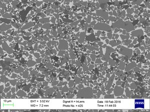
1000 mL (4 g of GO content) 250 mL (1 g of GO content) 5000 mL (20 g of GO content) 10000 mL (40 g of GO content) If you are developing a commercial application or wish to purchase a larger amount please contact: sales@kivoro.com Our graphene oxide is noted for its mechanical and thermal properties. The raw material - graphite - is chemically processed to obtain monolayer flakes of graphene oxide. Properties - Form: Dispersion of graphene oxide sheets - Particle Size: - D90 5-7 μm - D50 2-4 μm - D10 1-2 μm - Color: Yellow-brown - Odor: Odorless - Dispersibility: Polar solvents - Solvent: Water - pH: 1,8 - 2,5 - Concentration: 0.4 wt% - Monolayer content (measured in 0.05 wt%): 95% () - The Graphene Oxide weight content is guaranteed - The dispersion volume is approximated () 0.4% wt%concentration tends to agglomerate the GO flakes and dilution followed by slight sonication is required in order to obtain a higher percentage of monolayer flakes. Elemental Analysis - Carbon: 49 – 56% - Hydrogen: 1 – 2% - Nitrogen: 0 – 1% - Sulfur: 2 – 3% - Oxygen: 41 – 50% Quality control Our Graphene Oxide is subjected to a rigorous QC in order to ensure a high quality and reproducibility. - Amount of residue on evaporation - pH control - Elemental Analysis If your application requires more specific quality control, please do not hesitate to contact us. Applications Graphene/polymer composite materials, Batteries, Biomedical, Solar cells, Supercapacitors, Support for metallic catalysts, Low permeability materials, Biosensors, Multifunctional materials, Graphene research Publications “High‐Performance Graphene‐Based Cementitious Composites” Adv. Sci. 2019, 1801195. DOI:10.1002/advs.201801195 “Graphene oxide-carbon nanotubes aerogels with high sulfur loadings suitable as binder-free cathodes for high performance lithium sulfur batteries” Journal of Power Sources 412 (2019) 408–415. DOI:10.1016/j.jpowsour.2018.11.077 “Preparation of fabric strain sensor based on graphene for human motion monitoring” J Mater Sci 53, 9026–9033 (2018). DOI: 10.1007/s10853-018-2194-7 Downloads Data Sheet Graphene Oxide download MSDS Graphene Oxide download
CATEGORY
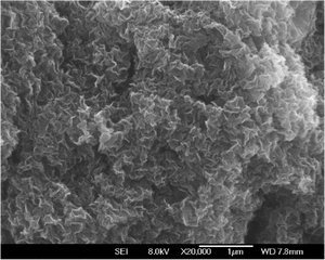
Reduced Graphene Oxide (rGO) is obtained by reducing Graphene Oxide (GO). It can be done chemically, thermally or via irradiation (UV or IR) to get a powder form. The great electrical conductivity of this product is an important feature in some research projects. Properties - Form: Powder - Reduction method: Chemically reduced - Particle Size: - D90 10-15 μm - D50 4-6 μm - D10 1-3 μm - Color: Black - Odor: Odorless - Solubility: Insoluble - Dispersability: It can be dispersed at low concentrations (<0.1mg/mL) in NMP, DMSO, DMF - Humidity (Karl Fisher, TGA): <1% - Electrical Conductivity: 667 S/m () - Specific Surface Area: 423 – 498 m2/g - Apparent Density: 0.20-0.30 g/cm3 () Measured in a 20nm film thickness Elemental Analysis - C (%): 80 – 87% - H (%): 0 – 1% - N (%): 0 – 1% - S (%): 0 - 1% - O (%): 13 – 17% Quality control Our Reduced Graphene Oxide is subjected to a rigorous QC in order to ensure a high quality and reproducibility. - Elemental Analysis If your application requires more specific quality control, please do not hesitate to contact us. Applications Biomedical, Batteries, Printable graphene electronics, Supercapacitors, Graphene research. Publications "Drop-coated reduced-GO thin film as counter electrode in DSSC" 2018 J. Phys.: Conf. Ser. 1080 012025. DOI:0.1088/1742-6596/1080/1/012025 "Platinum nanoparticles homogenously decorating multilayered reduced graphene oxide for electrical nanobiosensor applications" Thin Solid Films 658, 2018, 54-60. DOI: 10.1016/j.tsf.2018.05.032 "Dynamic Air-Brush Deposition Method for the New Generation of Graphene Based Supercapacitors" DOI:10.1557/adv.2018.65 Downloads Data Sheet rGO download MSDS rGO download If you are developing a commercial application or wish to purchase a larger amount please contact: sales@kivoro.com 3 g / 10 g / 50 g / 100 g
CATEGORY
