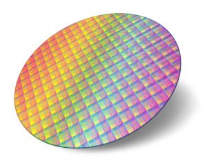
IXRF Systems’ ATLAS SEMI can analyze for: - bump inspection - CMOS image sensors (CIS) - corrosion resistance coating - Cu CMP control at BEOL - film stack - light elements - metal film stack composition such as CIGS - multi-stack structures - Pb measurement for Whiskers - redistribution layer (RDL) - Sn/Ag Bump/Pillar measurements - sputtering targets - thermal barrier coating - thick mono-layers - thickness and composition control - thin Film/Coating thickness measurements - ultra thin films - under bump metallization (UBM) - wafer-level packaging (WLP) IXRF Systems offers a 5µm spot size, the smallest on the market, allowing for extremely high resolution maps, analysis of small leads or pillars. IXRF Systems’ powerful software can be used to quickly identify, measure, and analyzed multiple solder bumps on a board. Quantitative analysis was done on one of the SnPb solder bumps in the center trio section, circled portion in the elemental map to the right. Below is an elemental map of a large area of a wafer with pillars, collected with a 5µm spot size.
