By micro resist technology GmbH
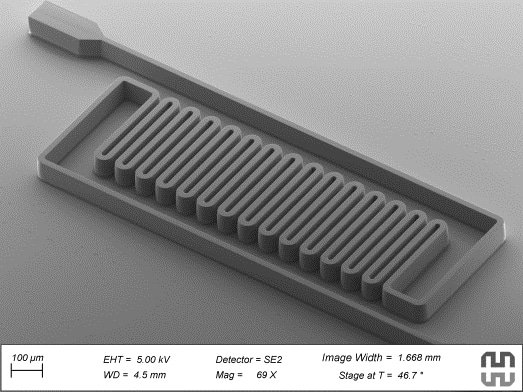
Unique Features - Specifically designed for exposure wavelengths above 400 nm - Suitable for DLW (e.g. @ 405 nm) & 2PP - High sensitivity - Excellent thermal and chemical stability - High wet and dry etch stability Applications - Fast and contactless prototyping by DLW & 2PP - Etch mask for wet and dry etch processes - Mould for electroplating - Mould for stamp fabrication by thermal or UV moulding - Optical applications in micro systems technology For Direct Laser Writing (DLW) @ 405 nm & Two Photon Polymerization (2PP) mr-DWL - Negative Tone Photoresist Series Resist mr-DWL 5, mr-DWL 40, mr-DWL 100 Film Thickness [µm] Spin Coating @ 1000 - 6000 rpm: 3 - 15, 10 - 100, 20 - 150 dyn. Viscosity [mPas] (@ 25°C): 360 @ 1000 s-1, 5.900 @ 150 s-1, 32.000 @ 40 s-1 Prebake 90 - 100 °C Spectral Sensitivity 350 nm - 410 nm i-line/ h-line Exposure dose @ 365 nm (Broadband exposure) 200 - 700 mJ/cm2; @ 405 nm 100 - 800 mJ/cm2 Post exposure bake (PEB) 75 - 100°C Developer mr-Dev 600 (solvent based) Remover mr-Rem 700 (NMP & NEP free), mr-Rem 500 (NMP free), O2-Plasma Recommended process chemicals: Thinner: no thinner available Developer: mr-Dev 600 (solvent based) Remover: mr-Rem 700 (NMP & NEP free), mr-Rem 500 (NMP free), O2-Plasma
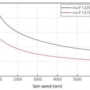
ma-P 1200G is a positive tone photoresist series specifically designed for the requirements of greyscale lithography. Standard binary lithography is also possible. Photoresist series for greyscale lithography Unique Features: - Reduced contrast - Film thickness up to 60 µm and higher - 50-60 µm depth range of the patterns possible in greyscale lithography - Spectral sensitivity 350…450 nm - High intensity laser exposure possible without outgassing - Aqueous alkaline development, for greyscale lithography with TMAH based developers, for standard binary lithography also with metal ion bearing developers - Suitable for electroplating - Suitable for dry etch processes e.g. with CHF3, CF4, SF6 - Suitable for pattern reflow after standard binary lithography Applications: - Use of manufactured 3D patterns in micro-optics, MEMS and MOEMS, displays - Pattern transfer by UV moulding, Etching, Electroplating Resist: ma-P 1215G, ma-P 1225G, ma-P 1240G, ma-P 1275G Film Thickness [µm] spin coating @ 3000 rpm: 1.5, 2.5, 4.0, 9.5 (up to 60 µm @ lower spin speeds) dyn. Viscosity [mPas] (typical values @ 25 °C, 1000 s-1): 21, 51, 122, 900 Prebake: 100–105°C, 100–105°C (9.5µm), 100°C (30 µm), Temperature ramp up to 100°C (60 µm) Spectral Sensitivity: 350 - 450nm; i-line - 365 nm; h-line - 405 nm; g-line 436 nm Exposure Dose Hg lamp @ 365 nm, Laser direct writing: 1 - 60 µm film thickness; 60 - 5000 mJ/cm² (Standard binary lithography); 10 - 350 ms/ spot (Greyscale lithography) Developer: mr-D 526/S, ma-D 532/S (TMAH based) for greyscale lithography; ma-D 331 (NaOH based) for standard binary lithography Remover: mr-Rem 700 (NMP & NEP free); mr-Rem 500 (NMP free); ma-R 404/S (strongly alkaline) Recommended process chemicals: Thinner: ma-T 1050 Developer: mr-D 526/S, ma-D 532/S (TMAH based) for greyscale lithography; ma-D 331 (NaOH based) for standard lithography Remover: mr-Rem 700 (NMP & NEP free); mr-Rem 500 (NMP free); ma-R 404/S (strongly alkaline)
CATEGORY
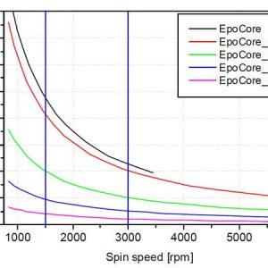
EpoCore & EpoClad series Unique Features - Standard UV lithography & PCB technology processing - UV patterning of core and cladding - High transmittance @ 850 nm - High heat ( 230 °C) and pressure resistance - Tunable refractive index (core/ cladding) Applications - Optical SM & MM polymer waveguides - Biosensors (multifunctional systems) - Microfluidics For manufacture of optical single mode (SM) & multi mode (MM) polymer waveguides EpoCore & EpoClad - Negative Tone Photoresist Series EpoCore Resist EpoCore 2 EpoCore 5 EpoCore 10 EpoCore 20 EpoCore 50 Film Thickness [µm] Spin Coating 2 @ 3000 rpm 5 @ 3000 rpm 10 @ 3000 rpm 20 @ 3000 rpm 50 @ 1500 rpm dyn. Viscosity [mPas] (@ 25°C) 85 @ 1000 s-1 350 @ 1000 s-1 1.130 @ 1000 s-1 2.800 @ 1000 s-1 10.100 @ 150 s-1 Prebake 90 - 100°C Spectral Sensitivity i-line - 365nm Exposure Dose @ 365 nm UV mercury lamp (broadband exposure), UV-LED 150 - 600 mJ/cm 2 Post exposure bake (PEB) 85°C Developer mr-Dev 600 (solvent based) Hardbake 120 - 140 °C (optional) Remover mr-Rem 700 (NMP & NEP free), mr-Rem 500 (NMP free), O 2-Plasma EpoClad Resist EpoClad 2 EpoClad 5 EpoClad 10 EpoClad 20 EpoClad 50 Film Thickness [µm] Spin Coating 2 @ 3000 rpm 5 @ 3000 rpm 10 @ 3000 rpm 20 @ 3000 rpm 50 @ 1700 rpm dyn. viscosity [mPas] (@ 25°C) 80 @ 1000 s-1 330 @ 1000 s-1 1.000 @ 1000 s-1 2.300 @ 1000 s-1 9.500 @ 150 s-1 Prebake 120°C Spectral Sensitivity i-line - 365nm Exposure Dose @ 365 nm UV mercury lamp (broadband), UV-LED 200 - 500 mJ/cm 2 Flood exposure for cladding Post exposure bake (PEB) 120°C Developer mr-Dev 600 (solvent based) Hardbake 120 - 140 °C (optional) Remover mr-Rem 700 (NMP & NEP free), mr-Rem 500 (NMP free), O 2-Plasma Recommended process chemicals: Thinner no thinner available Developer mr-Dev 600 (solvent based) Remover mr-Rem 700 (NMP & NEP free), mr-Rem 500 (NMP free), O2-plasma
CATEGORY
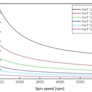
Positive Photoresist Series and Thick Film Photoresists for UV lithography Unique Features - Film thickness up to 60 μm in one spin-coating step - Broadband-, g- and i-line exposure - High stability in acid and alkaline plating baths - High dry and wet etch resistance - Good thermal stability of the resist patterns attainable - Aqueous alkaline development - Side wall angle up to 87° with mask aligner broadband exposure - Suitable for pattern reflow Applications - Etch mask - metals and semiconductors - Mould for electroplating - Fabrication of micro optical components,e.g. micro lenses by pattern transfer from reflowed resist patterns - Mask for ion implantation ma-P 1200 series and ma-P 1275 & ma-P 1275HV for microsystems technology and microelectronics Resist ma-P 1205 ma-P 1210 ma-P 1215 ma-P 1225 ma-P 1240 ma-P 1275 ma-P 1275HV Film Thickness [µm] spin coating @ 3000 rpm 0.5 1.0 1.5 2.5 4.0 7.5 (up to 40 µm at lower spin speed) 11 (up to 50 µm at lower spin speeds) dyn. Viscosity [mPas] (@ 25 °C, 1000 s-1) 5 12 22 50 125 460 1100 Prebake 100 - 105°C Spectral Sensitivity 350 - 450nm i-line - 365 nm; h-line - 405 nm; g-line 436 nm Exposure Dose Hg lamp @ 365 nm UV-LED monochromatic 35 - 4000 mJ/cm 2 (0.5 - 50 µm film thickness) 1000 - 4000 mJ/cm 2 ( 10 µm film thickness) Developer mr-D 526/S (TMAH based) - for greyscale lithography ma-D 331 (NaOH based) - for standard binary lithography Remover mr-Rem 700 (NMP & NEP free) mr-Rem 500 (NMP free) ma-R 404/S (strongly alkaline) Recommended process chemicals: Thinner ma-T 1050 Developer mr-D 526/S (TMAH based) ma-D 331 (NaOH based) Remover mr-Rem 700 (NMP & NEP free) mr-Rem 500 (NMP free) ma-R 404/S (strongly alkaline)
CATEGORY
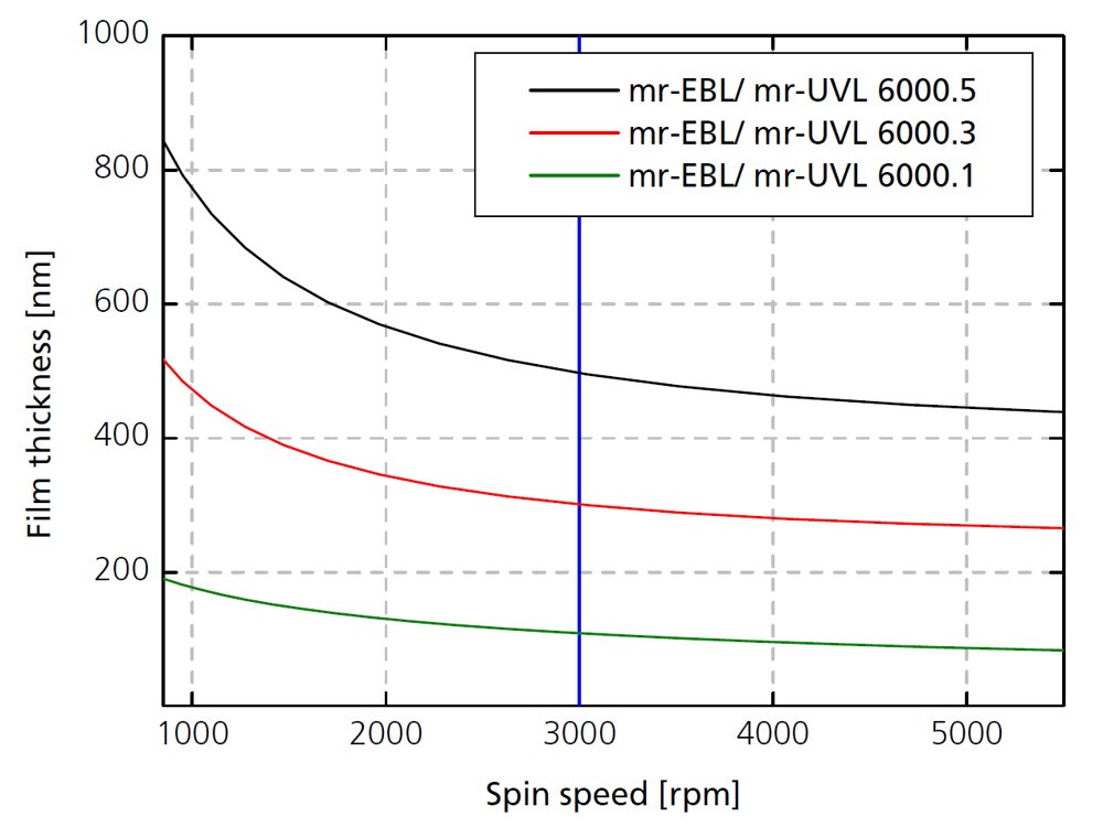
mr-EBL 6000 - Negative Tone Resist Series Unique Features E-beam sensitivity: 2 - 6 μC/cm2 @ 30 keV 2 - 6 μC/cm2 @ 50 keV 8 - 15 μC/cm2 @ 100 keV Post exposure bake (PEB) necessary Development in organic solvents Excellent thermal stability of the resist patterns High wet and dry etch resistance Resolution capability: 80 nm Applications Use in micro- and nanoelectronics Manufacturing of semiconductor devices Mask for etching, e.g. of Si, SiO2, Si3N4 or metals Generation of stamps with nanopatterns High E-beam sensitivity Resist mr-EBL 6000.1 mr-EBL 6000.3 mr-EBL 6000.5 Film Thickness [µm] Spin Coating @ 3000 rpm 0.1 0.3 0.5 dyn. Viscosity [mPas] (@ 25 °C, 1000 s-1)1.4 2.3 3.4 Prebake 90°C Sensitivity E-beam Exposure Dose E-beam @ 30 keV E-beam @ 50 keV E-beam @ 100 keV 2 – 6 µC/cm 2 2 – 6 µC/cm 2 8 – 15 µC/cm 2 Post exposure bake (PEB)100 - 120°C Developer mr-Dev 600 (solvent based) Remover mr-Rem 700 (NMP & NEP free) mr-Rem 500 (NMP free) O 2-Plasma Recommended process chemicals: Thinner ma-T 1045 Developer mr-Dev 600 (solvent based) Remover mr-Rem 700 (NMP & NEP free) mr-Rem 500 (NMP free) O2-Plasma Mask for etching
CATEGORY
