By IMT Masken und Teilungen AG
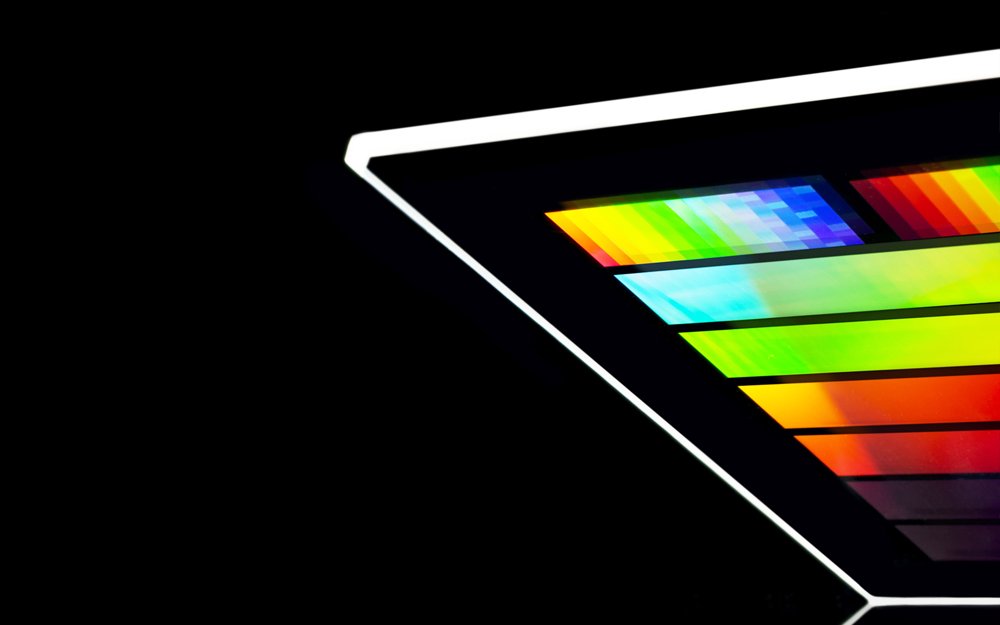
Large-scale: binary amplitude and phase gratings for the spectral decomposition and spatial separation of optical radiation Optical gratings are used extensively in optoelectronics. They are put to use wherever spectral decomposition or spatial separation of optical radiation is required. In contrast to conventional production technologies, IMT has the capability to structure optical gratings on a large scale. - Area: 5 x 5 inches - Material: Quartz, B270, N-BK7, D263, Borofloat, Zerodur - Thickness: 0.3 mm–10 mm - Structure size: > 150 nm - Amplitude or phase gratings Applications: - Telecom/datacom - Optical spectroscopy - Beam formation - Measurement technology - Beam splitters
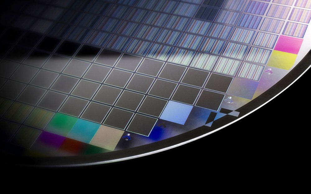
Maximum brilliance: microstructured dielectric and metallic coatings Optical components such as lenses, mirrors, beam splitters and gratings can mostly be used in photonics, the semiconductor industry or medical technology if they have been fully coated. Depending on the application, these coatings have a wide range of functions throughout the system. IMT specialises in microstructuring and combining dielectric coatings with metal or electrically conductive coatings. In addition to well-known applications, such as the Bayer filter, interesting new applications become available for our customers. Solderable coatings allow for easy integration at chip or wafer level and can be used as electrodes. Structured ITO coatings, which have both an optical and electronic function, round off our varied range of products. For you, this means: - Complete solutions from a single source - Maximum accuracy of structures - Quick lead times - A lean supply chain - Cleaner processes (clean room conditions ISO 14644-1, class 5 and 6) We would be very happy to provide you with customer-specific solutions which can be integrated into your production process. Slit projection – microstructured graduated filter for structured lighting: Our elements are used for 3D measurement using slit projection: An image is projected onto the object with a defined light-dark distribution and the signal reflected by the object is recorded with a camera. The position of the object points is calculated, in the same way as a triangulation sensor, from the angle between the direction of light and direction of observation. The range of applications is just as broad as the evaluation algorithms for the generation of the digital 3D model. It covers everything from automotive and aircraft construction to dental technology and reverse engineering right through to forensics. Checkerboard pattern – structured lighting in the intraoral scanner: The elements are characterised by the combination of metallic microstructures with an anti-reflective coating on both sides. This highlights surface defects and steep edge transitions (light-dark) in particular. Substrate: Fused silica, B270, Borofloat, D263, other materials on request Thickness: 0.3 mm–10 mm Coating material: Chrome, IMT-BC Structure sizes: 2 µm Tolerance: ±0.5 µm Position accuracy: < ±0.5 µm Optical density of the metallic coating: 3 AR coating: on request
CATEGORY
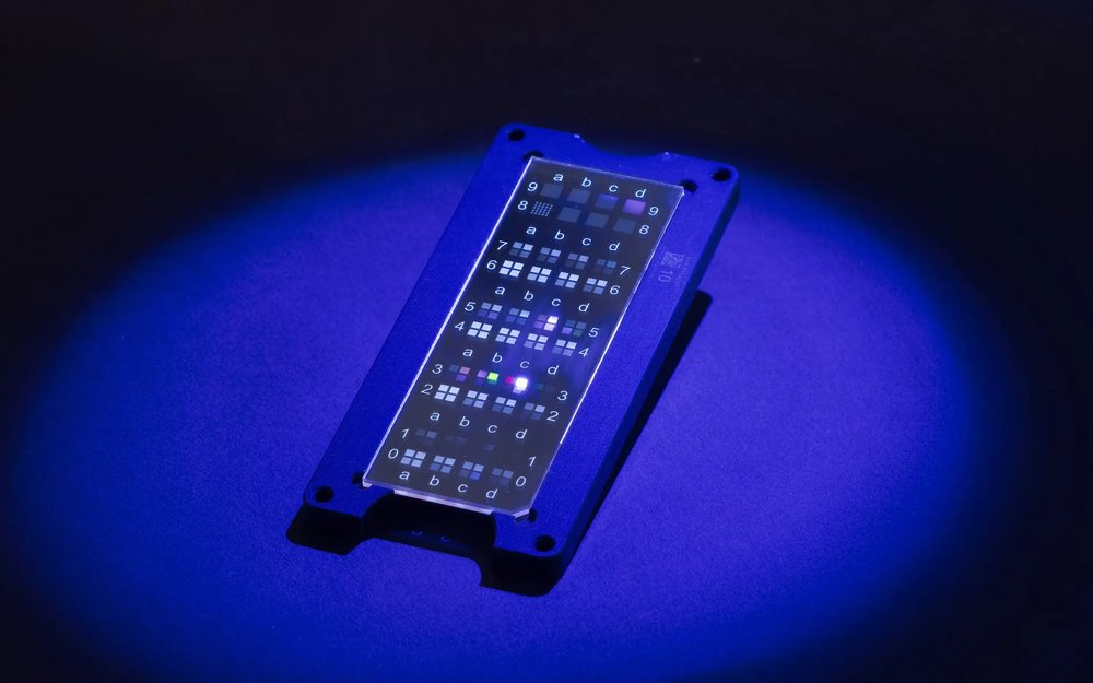
Fluorescent targets are used for the precise calibration and characterization of fluorescence microscopes. They enable reproducible x/y/z positioning as well as the calibration of sensitivity and resolution. Based on photoluminescent thin films in combination with high-precision apertures on glass, they generate defined and stable emission patterns. By carefully selecting the coatings, brightness, robustness, and durability can be optimized, resulting in long-lasting reference standards for applications in life sciences and diagnostics. These solid-state solutions provide a robust and maintenance-free alternative to conventional liquid or particle-based calibration methods. Their high photostability and resistance to photobleaching ensure consistent performance even under intense illumination conditions. In addition, the structures can be precisely tailored in terms of geometry, emission wavelength, and intensity, allowing seamless integration into a wide range of microscopy systems. This makes them ideally suited not only for routine calibration tasks, but also for system validation, performance benchmarking, and advanced imaging applications. Datasheet Fluorescent Solid State Targets
CATEGORY
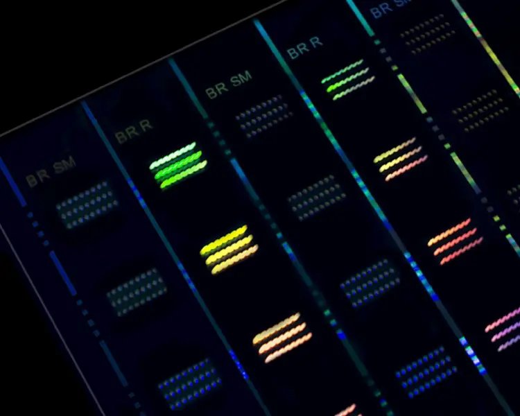
Highest precision: High refractive index planar waveguides (PWG) have a wide range of uses in chemical analytics and in the telecom/datacom sector for the coupling and decoupling of optical signals. IMT produces customer-specific waveguides including the coupling gratings on the basis of tantalum pentoxide (Ta 2 O 5) and other coating materials. Building on this foundation, IMT leverages its extensive expertise in thin-film deposition and microstructuring to achieve exceptional precision and reproducibility in the fabrication of planar waveguides. The controlled application of high-quality materials such as Ta 2 O 5 allows for finely tuned optical properties, including refractive index uniformity and low propagation losses. By integrating tailored coupling gratings directly into the waveguide structures, IMT ensures highly efficient in- and out-coupling of optical signals adapted to specific wavelengths and system requirements. This precise and flexible manufacturing approach enables reliable, application-specific solutions for demanding environments in both chemical analytics and telecom/datacom, where performance, stability and miniaturisation are key.
CATEGORY
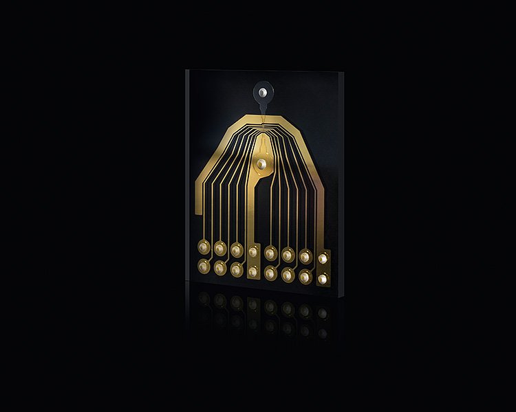
Highly functional: microfluidic biochips for the biotechnology of the future IMT is one of the pioneers in the area of microfluidic glass components and biochips. As early as 1990, our technology allowed for the development of the first µTAS chip by Andreas Manz. The combination of automated semiconductor processes with existing MEMS technology opens up brand-new possibilities for our customers. There are even new fields of application in cost-sensitive areas, in which it has not previously been possible to consider optical glass. - Lab-on-a-chip - DNA analysis - Microreactors - Droplet generators - Impedance chips - Organ-on-a-chip - Micro-, nano-arrays - Single cell detection - High throughput screening Etched microchannels, bores (TGV), structured metal and dielectric coatings, electronic conductors (electrodes), optical gratings, concave structures (dot arrays) and planar waveguides Substrate: Fused silica, B270, Borofloat, D263, other materials on request Thickness: 0.3 mm–10 mm Structure sizes: ≥ 2 µm Tolerance: ±0.5 µm Position accuracy: < ±0.5 µm
CATEGORY
