Prices: Box of 10 cantilevers = 280€ Box of 20 cantilevers = 500€ Box of 50 cantilevers = 1150€ Unique advantages: - Tapered Streamlined Long Tip - Vertical sidewall chip for safe handling - Tip view Applications - Soft tapping mode / Force modulation mode - Compatible for narrow trenches or high roughness samples imaging
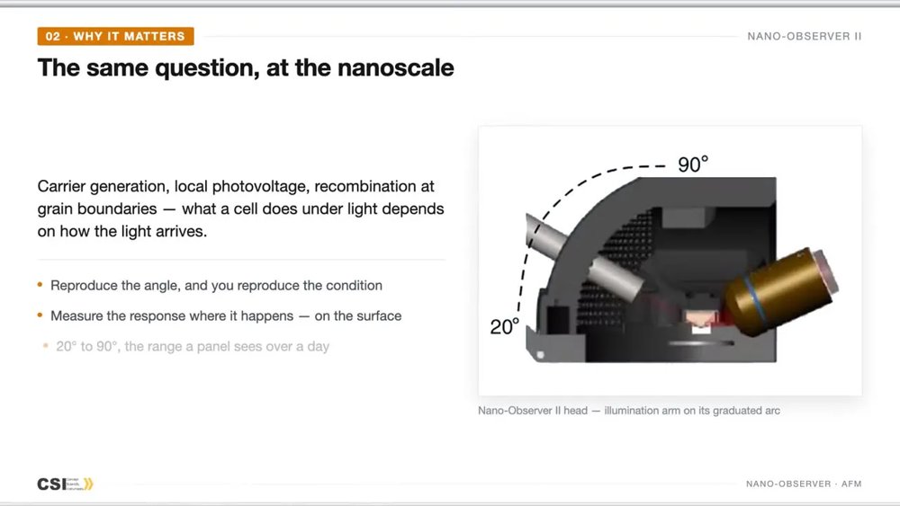
100 × 100 µm XY scan range 15 µm Z range 24-bit Galaxy USB controller 20+ modes on one head, upgradable Designed for demanding research, simple to use every day User-Friendly Design - Top and side views of the tip/sample area for efficient pre-approach process - Compact AFM head with optional Pre-Alignment tip/laser holder AutoScan Software: Easier & Faster Automated Scan - Auto approach (automated fast and gentle final approach) - Autogain: realtime active AFM feedback gains - Setpoint conditions: preset Setpoints (For Soft, Medium or Hard interaction) High-Performance Scanning - Low-noise, high-resolution scanning capabilities - Large-small area scans without changing scan head - Consistent resolution across all scan sizes Advanced Technology Integration - The New Galaxy USB 24-bit low noise AFM controller - High quality built in lock-ins - Phase, PFM, EFM, KPFM… - Key modes: HD-KFM and ResiScope for high-resolution imaging An open head, built for light The illumination arm sweeps the light from 20° to 90° — the same range the sun covers over a day — so photovoltaic samples are measured under the conditions they see in the field. - Continuously adjustable on a graduated arc - Locked at any angle onto the sample - Open head for UV, IR and Raman integration Nano-Observer II specifications Scanner Specifications - XY Scan Range: 100 μm × 100 μm (±10%) - Z Range: 15 μm (±10%) - XY Drive Resolution: 0.06 Angströms - Z Drive Resolution: 0.006 Angströms Imaging Modes - Standard Modes: Contact, Resonant, Soft Intermittent Contact - Magnetic Modes: Magnetic Force Microscopy, Variable Magnetic Field Module - NanoMechanical Modes: Soft MEKA, Force Modulation, Nano-Indentation, Force Spectroscopy, Friction (LFM) - Electrical Modes (AC): HD-KFM III, Kelvin Force Microscopy (double-pass), Electrostatic Force Microscopy - Electrical Modes (DC): ResiScope™ III, Soft ResiScope, Conductive AFM, Scanning Microwave Impedance, Piezo Response Force Microscopy Electrical Measurements - ResiScope Range: 10² to 10¹² ohms - Voltage Range: ±10 V (adjustable) Controller & Data Acquisition - Controller Resolution: 24-bit - Built-in Lock-in Amplifier: Up to 6 MHz - Maximum Data Points: 8192 × 8192 Sample Stage - Sample Size: Up to 52 mm (2 inches) diameter - Sample Height: Up to 20 mm - Motorized Sample Approach: 20 mm range Environmental Control - Temperature Range: -40°C to 450°C (with optional module) - Humidity Control & Gas Control: Optional - Liquid Cell: Available for fluid imaging Electrochemical AFM (EC-AFM) - Electrochemical Cell: Three-electrode configuration - Potential Range: ±10 V Software - OS Compatibility: Windows 10/11 - AutoScan Feature: Automated imaging with three-click operation - Real-time Data Processing & Analysis FAQ What is the Nano-Observer II? The Nano-Observer II is an advanced Atomic Force Microscope (AFM) manufactured by CSInstruments (France). It is designed for both expert researchers and beginners, offering a wide range of nanoscale imaging and characterization capabilities. Key differentiators include the proprietary HD-KFM III module for single-pass surface potential mapping, the ResiScope III module for 10-decade electrical measurements, and the Soft Intermittent Contact (Soft-IC) mode for non-destructive measurements on delicate samples. The system features a 24-bit Galaxy USB controller, scan range of 100 × 100 µm in XY and 15 µm in Z, and is compatible with optical techniques including UV, IR, and Raman spectroscopy. What AFM modes are available on the Nano-Observer II? The Nano-Observer II supports a comprehensive set of AFM modes: standard imaging modes (Contact, Resonant, Soft Intermittent Contact); electrical AC modes (HD-KFM III, HD-KFM I, standard KFM, EFM, PFM); electrical DC modes (ResiScope III, Soft ResiScope, Conductive AFM, Scanning Microwave Impedance); nanomechanical modes (Soft MEKA, Force Modulation, Nano-Indentation, Force Spectroscopy, Friction/LFM); magnetic modes (MFM, Variable Magnetic Field Module); thermal modes (Scanning Thermal Microscopy, Peltier/Heating stages); and environmental modes (liquid cell, electrochemical cell, gas/humidity control, glove box compatibility). What is the scan range of the Nano-Observer II? The Nano-Observer II has an XY scan range of 100 µm × 100 µm (±10%) and a Z range of 15 µm (±10%). XY drive resolution is 0.06 Ångströms and Z drive resolution is 0.006 Ångströms. The maximum data acquisition resolution is 8192 × 8192 points. The sample stage accepts samples up to 52 mm (2 inches) in diameter and up to 20 mm in height. What makes the Nano-Observer II different from competing AFM systems? Three proprietary technologies distinguish the Nano-Observer II: (1) HD-KFM III — a single-pass Kelvin Probe Force Microscopy module operating at 0.1–0.5 nm tip-sample distance, achieving 100–10,000× greater electrostatic sensitivity than standard lift-mode KFM; (2) ResiScope III — an electrical measurement module with 10-decade dynamic range (50 fA to 1 mA, 10² to 10¹² ohms) in a single scan pass, overcoming C-AFM saturation limitations; and (3) Soft Intermittent Contact (Soft-IC) mode — a third imaging paradigm combining contact and resonant mode advantages for non-destructive measurements on soft or fragile samples. The AutoScan software with three-click operation and automated gain adjustment further lowers the barrier for non-expert users. Can the Nano-Observer II be used with optical microscopy techniques? Yes. The Nano-Observer II has an open design that allows integration with optical microscopy techniques including UV, infrared (IR), and Raman spectroscopy. This enables correlated AFM and optical measurements on the same sample area, which is particularly useful for photovoltaic research, 2D material characterization, and biological imaging. Is the Nano-Observer II compatible with a glove box for air-sensitive samples? Yes. The Nano-Observer II can be operated inside a glove box with controlled gas atmosphere (e.g., N₂ or Ar) and humidity control. This is essential for characterizing air-sensitive materials such as lithium metal anodes, 2D materials, organic semiconductors, and perovskite photovoltaic films that degrade upon exposure to ambient atmosphere. What electrical measurement capabilities does the Nano-Observer II offer? The Nano-Observer II offers the most comprehensive electrical AFM suite in its class: AC electrical modes include HD-KFM III (single-pass surface potential, sub-nm tip distance), standard KFM (double-pass), EFM, and PFM. DC electrical modes include ResiScope III (50 fA–1 mA, 10 decades), Soft ResiScope (friction-free electrical measurement on fragile samples), Conductive AFM, and Scanning Microwave Impedance Microscopy (sMIM). The voltage range for electrical measurements is ±10 V. What is Soft Intermittent Contact (Soft-IC) mode on the Nano-Observer II? Soft Intermittent Contact (Soft-IC) is CSInstruments' third AFM imaging paradigm, alongside contact and resonant modes. It operates by making controlled, brief intermittent contact with the surface using Z-piezo movement, maintaining constant force during each measurement point before retracting. This eliminates lateral friction forces that can damage soft samples or degrade tip sharpness. Soft-IC enables Soft MEKA (stiffness, adhesion, Young's modulus), Soft ResiScope (electrical mapping on fragile conductors), Soft PFM, and Soft SThM on samples that would be damaged by standard contact or resonant mode AFM.
CATEGORY
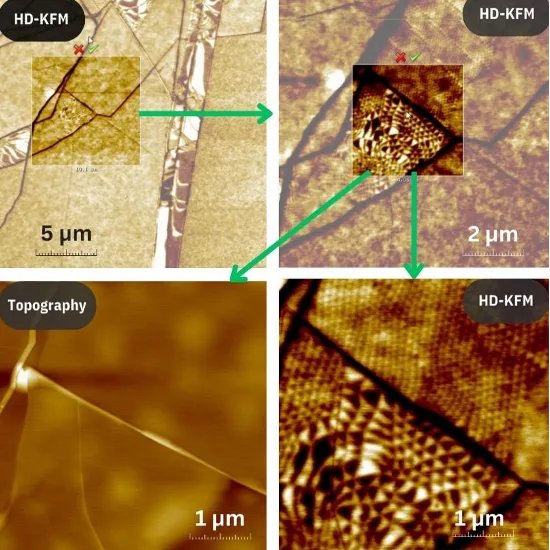
The CSInstruments Nano-Observer AFM series represents a quantum leap forward in nanoscale characterization, offering researchers unprecedented insights into the surface morphology and electrical properties of 2D materials at resolutions previously thought impossible. The CSInstruments Nano-Observer introduces HD-KFM technology through innovative signal processing and optimization. As demonstrated in comparison images, HD-KFM provides dramatically improved visualization of graphene layers. Standard KFM mode shows limited contrast between different layer thicknesses, while HD-KFM mode reveals precise layer boundaries and subtle electronic variations across the sample with exceptional clarity. Key advantages of HD-KFM include: - Operates at much higher frequencies (350-400 kHz vs ~17kHz) - 20 to 30 times more measurement cycles per scan - Enhanced sensitivity using eigenmode detection - One-click auto-tune algorithm for optimal settings - Sharp, accurate boundary mapping with exceptional clarity The practical implications are substantial. Researchers can now detect subtle electronic property variations at layer boundaries with unprecedented precision, identify defects and contamination at the nanometer scale, characterize heterojunctions with detail that was previously impossible, and accelerate materials development from fundamental research to functional devices. The Nano-Observer’s HD-KFM technology reveals these effects through surface potential mapping with unprecedented resolution. The system provides multi-scale characterization from large-scale domain structure analysis (5 μm scale) showing overall sample architecture, to mid-range detailed mapping (2 μm scale) of domain boundaries and transitions, down to high-resolution moiré pattern visualization with ~100 nm triangular domains at 1 μm scale. Beyond surface potential mapping, the Nano-Observer integrates Piezoresponse Force Microscopy (PFM) with HD-KFM, allowing researchers to correlate electronic properties via surface potential variations, structural properties through domain structure mapping, and electromechanical responses via PFM signal analysis. This multi-modal approach enables measurements on the exact same sample area with perfect spatial registration—a critical capability that was missing in conventional characterization workflows. The Nano-Observer AFM with HD-KFM provides unprecedented visualization of these layer-dependent variations, enabling researchers to precisely identify monolayer (1ML), bilayer (2ML), trilayer (3ML), and four-layer (4ML) regions, map work function differences across the sample with intuitive color contrast, detect sharp, well-defined interfaces between regions with different layer counts, and correlate electronic structure directly with layer thickness. The Nano-Observer system provides synergistic electrical characterization through the combination of ResiScope™ and HD-KFM technologies. ResiScope™ maps resistance across an exceptional range (10² to 10¹² Ω), clearly distinguishing between conductive and insulating regions and revealing how conductivity changes exponentially with layer thickness. Meanwhile, HD-KFM measures work function shifts with nanometer-scale resolution, maps charge distribution across different layer counts, and reveals systematic changes in surface potential with layer thickness. The CSInstruments Nano-Observer AFM Series represents a paradigm shift in nanoscale characterization technology. By integrating multiple advanced measurement techniques within a single platform, this system enables discoveries that would be impossible with conventional AFM approaches. Key advantages for researchers include unprecedented resolution with HD-KFM revealing electronic property variations at the nanometer scale, multi-modal analysis to correlate topography, electrical properties, and electromechanical responses, precision measurement with one-click optimization that eliminates manual tuning errors, quantitative data extraction of precise work functions, resistance values, and layer counts, and accelerated research that reduces characterization time while increasing data quality. Applications span across industries including quantum computing for characterizing moiré superlattices and correlated quantum states, nanoelectronics for optimizing 2D material transistors and interconnects, optoelectronics for developing next-generation photodetectors and light-emitting devices, energy storage for understanding electrode materials at the atomic scale, and sensors for designing ultra-sensitive chemical and biological detection systems. The Nano-Observer AFM series doesn’t just measure these materials—it reveals the fundamental relationships between structure and function that enable breakthrough innovations.
CATEGORY
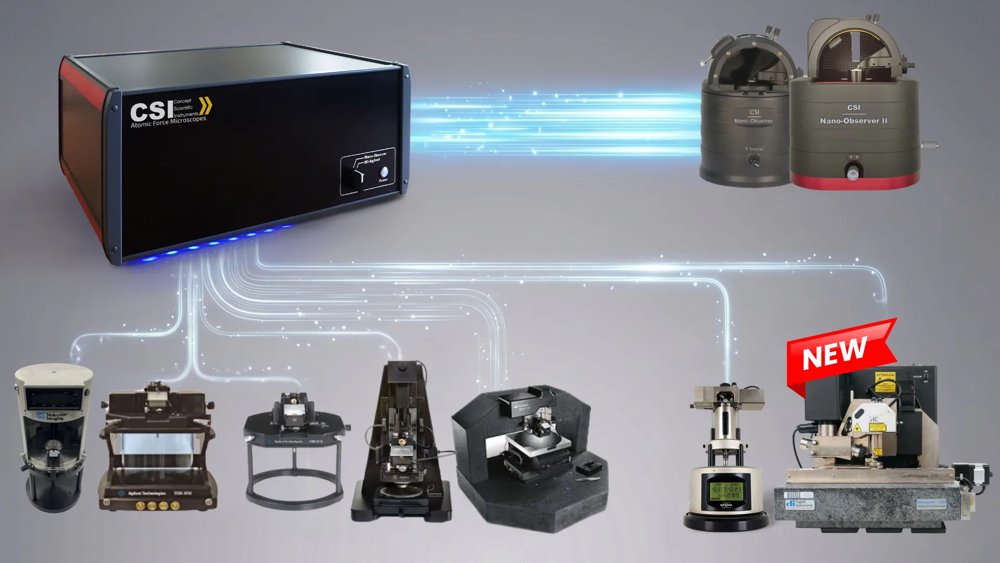
A Second Life For Your Existing AFM System Upgrade your AFM capabilities with the Galaxy Dual Controller: A breakthrough solution compatible with Multimode, Dimension D3000 & D3100, 5100, 5500, 5600LS, and 54xx AFM/STM platforms. This advanced controller system not only modernizes your existing microscope but also introduces enhanced functionality for expanded research applications. Seamless Compatibility - Technical expertise operating diverse AFM/SPM systems including Multimode AFM, Pico SPM (STM), Dimension 3000/3100 and Agilent/Keysight scanning probe microscopes (5100, 5500, 5600LS, and 54xx models) - Maintains existing modes: STM, Contact, AC, Phase, MFM, EFM, PFM, LFM, EC modes Advanced New Modes for your old AFM - HD-KFM: No lift, higher sensitivity & resolution - ResiScope & Soft ResiScope: Resistance & current measurements from 10² to 10¹² ohms and 50 fA to mA range, even on soft samples - Soft Interaction Control Mode: Measure adhesion, stiffness, Young's modulus with quantitative accuracy High-Performance Hardware - Real integrated lock-in for enhanced measurement capabilities - Low-noise electronics and power supply - USB 24-bit drive architecture for high resolution and smart integration AutoScan Features & NanoSolution Software - Auto tune - Auto approach - Auto gain - Predefined setpoint conditions - Point and Click to automatically navigate and start measurements - Automated positioning, mapping, and measurement routines - Full motorized XY stage control (when available) - Active gain optimization for improved stability User-Friendly Software - Intuitive NanoSolution interface - One-click mode selection and automatic electronics configuration - Guided workflow for efficient image acquisition - Auto-settings for quick results and expert controls for in-depth analysis AFM controller upgrade Upgrade the controller of an existing AFM The Galaxy Dual Controller is the AFM controller upgrade made by CSInstruments, a French manufacturer of atomic force microscopes. It replaces the controller and software of an existing microscope and drives its own head, scanner and stage: every mode the AFM already had is kept, and HD-KFM™, ResiScope™ and Soft Interaction Control are added. Compatible AFMs Original manufacturer | AFM model | Notes Bruker (Veeco / Digital Instruments) | MultiMode | all standard modes and STM Bruker (Veeco / Digital Instruments) | Dimension 3000 and 3100 | full control, including auto approach and the motorized XY stage Molecular Imaging / Agilent / Keysight | 5100 and 5500 | including electrochemistry Molecular Imaging / Agilent / Keysight | 5400 and 5420 | Molecular Imaging / Agilent / Keysight | 5600LS | Molecular Imaging | PicoSPM (STM) | Kept from the original AFM - STM - Contact mode - AC (resonant) mode - Phase imaging - MFM and EFM - PFM - Lateral force (LFM) - Electrochemistry (EC) Added by the upgrade - HD-KFM™ — single-pass Kelvin probe force microscopy, no lift, higher sensitivity and resolution - ResiScope™ and Soft ResiScope™ — resistance from 10² to 10¹² Ω and current from 50 fA to mA, also on soft samples - Soft Interaction Control — adhesion, stiffness and Young’s modulus - NanoSolution software with AutoScan — auto tune, auto approach, auto gain, point-and-click navigation - 24-bit USB drive electronics with an integrated lock-in and low-noise high voltage How the upgrade is done CSInstruments installs the controller on site and trains the users, as at the Universidade Federal do ABC in Brazil on an Agilent 5500. The microscope stays the one the lab knows; the electronics, software and modes are new. Upgrade your research capabilities HD-KFM Mode - Achieve higher sensitivity and resolution in Kelvin Probe Force Microscopy - Perfect for advanced materials research, including 2D materials like graphene ResiScope Mode - Wide-range resistance and current mapping - Ideal for semiconductor research, dopant profiling, and nanoelectronics Soft Intermittent Contact Mode - Non-destructive analysis of soft and delicate samples - Quantitative measurements of mechanical properties Why upgrade with the Galaxy Dual Controller? Cost-Effective Significantly enhance your AFM capabilities without the expense of a new system Expand Research Horizons Access new modes and measurements previously unavailable on your AFM Improve Efficiency User-friendly software streamlines your workflow and reduces learning curve Future-Proof Your Lab Stay competitive with cutting-edge AFM technology Galaxy Dual Controller specifications - XY Drive Resolution: 24-bit control - 0.06 Å - Z Drive Resolution: 24-bit control – 0.006 Å - Ultra-Low Noise HV: Typ: <0.01 mV RMS - 6 DAC Outputs: 6 D/A Converters – 24 bit (XYZ drive, bias, aux…) - 8 ADC Inputs: 8 A/D Converters – 16 bit - Data Points: Up to 8192 - Integrated Lock-in: Up to 6 MHz (software limited), 2nd lock-in (6 MHz-optional) - Interface: USB 2.0 - Power: AC 100 – 240 V - 47-63 Hz - OS Compatibility: Windows 10, 11 Frequently Asked Questions Which companies offer controller upgrades for existing AFMs? CSInstruments, a French manufacturer of atomic force microscopes, makes the Galaxy Dual Controller: a controller upgrade for Bruker MultiMode and Dimension 3000/3100 AFMs and for Molecular Imaging, Agilent and Keysight 5100, 5400/5420, 5500, 5600LS and PicoSPM systems. Can an old Bruker MultiMode AFM be upgraded with a new controller? Yes. The Galaxy Dual Controller drives the MultiMode head and scanner, keeps its existing modes (STM, contact, AC, phase, MFM, EFM, PFM, LFM) and adds HD-KFM, ResiScope and Soft Interaction Control. Can an Agilent or Keysight 5500 AFM be upgraded? Yes. The Galaxy Dual Controller operates the MI, Agilent and Keysight 5100, 5400/5420, 5500 and 5600LS AFMs. The Universidade Federal do ABC in Brazil upgraded its Agilent 5500 with on-site installation and hands-on training. Is the Dimension 3100 fully controlled after the upgrade? Yes. The Galaxy Dual Controller controls the Dimension 3000 and 3100 completely, including automated tip engagement (auto approach) and the motorized XY stage, from the new software. Does a controller upgrade keep the modes the AFM already has? Yes. STM, contact, AC, phase, MFM, EFM, PFM, LFM and electrochemistry are kept; HD-KFM, ResiScope, Soft ResiScope and Soft Interaction Control are added. Can the Galaxy Dual Controller run STM (scanning tunneling microscopy)? Yes. STM is among the modes kept when an existing system is upgraded, and the Molecular Imaging PicoSPM (STM) is on the compatibility list, together with the MultiMode, Dimension 3000/3100 and Agilent / Keysight 5100, 5500, 5400/5420 and 5600LS. Don't let your valuable AFM become obsolete. Upgrade with the Galaxy Dual Controller and unlock new research possibilities today.
CATEGORY
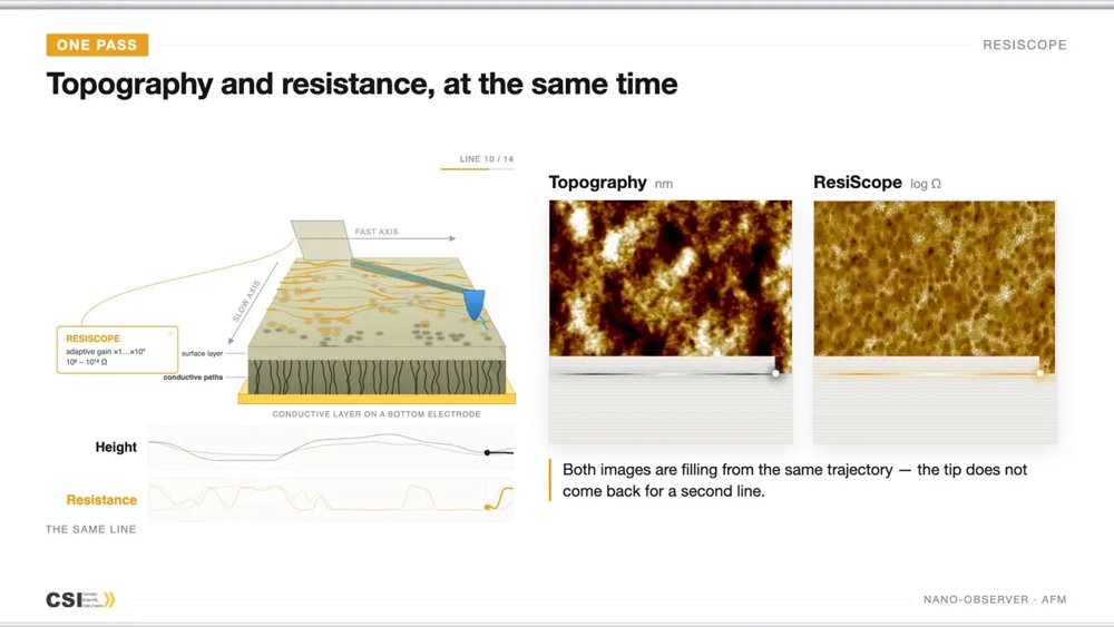
When one current range is not enough: ResiScope™ Conventional conductive AFM measures the current with one amplifier whose gain is fixed before the scan, so only about four decades are read correctly. Highly conductive areas saturate the amplifier — often around 10 nA — while insulating areas disappear in the noise. On heterogeneous samples such as battery electrodes, solar cells, composites or 2D materials the image is only partly quantitative, and capacitive effects and surface charging add artefacts. ResiScope™ is CSInstruments' answer. It works like C-AFM — a conductive tip, a bias voltage, contact with the sample — but a DSP-controlled amplifier re-chooses its gain at every measured point. Resistance from 10² to 10¹² Ω and current from fA to µA are measured in the same scan, together with the topography, with no saturation, no manual range switching and real-time current protection for tip and sample. - 10 decades in one scan — 10²–10¹² Ω and fA to µA, where standard C-AFM covers about four. - No clipped domains, no charging baseline — conductive and insulating areas are both quantitative. - Fragile samples — Soft ResiScope™ measures in intermittent contact, without shear. - Surface potential on the same area — combine with HD-KFM™, single-pass Kelvin probe force microscopy (KPFM), to correlate conductivity and work function. - Where — ResiScope™ III on the Nano-Observer II, ResiScope™ II on the Nano-Observer One Plus, and on existing AFMs with the Galaxy Dual Controller. How does ResiScope™ differ from standard C-AFM? ResiScope™ goes beyond C-AFM in three fundamental ways. First, it measures resistance directly and quantitatively at every pixel — not just current. Second, its 10-decade dynamic range (10² to 10¹² Ω, fA to µA) covers both conductive and insulating regions in a single scan without saturation. Third, its Soft-ResiScope mode enables measurements at very low contact forces, preserving fragile samples that standard C-AFM would damage. Can ResiScope™ replace C-AFM entirely? Yes — ResiScope™ is a direct upgrade to standard C-AFM. It performs everything C-AFM does, and adds direct resistance mapping, 10× wider dynamic range, real-time auto-gain control, and soft-mode operation. Researchers who switch from C-AFM to ResiScope™ gain quantitative resistance data and full dynamic range without changing their workflow. What is the dynamic range of ResiScope™ compared to other C-AFM systems? ResiScope™ covers 10 full decades of resistance — from 10² to 10¹² Ω — and detects currents from femtoamperes (fA) to microamperes (µA) in a single pass. Standard C-AFM systems typically cover 4–5 decades and require manual gain switching or multiple scans. ResiScope™'s real-time DSP auto-gain system handles the full range automatically. Which materials and applications is ResiScope™ best suited for? ResiScope™ is optimized for solid-state batteries (mapping both conductive active particles and resistive binders/electrolytes), semiconductors and nanoelectronics (failure analysis, leakage current), 2D materials (graphene, MoS₂, hBN), photovoltaic cells (grain boundary analysis, defect mapping), organic electronics, thin films, and polymers. Any application requiring electrical characterization across a wide conductivity range benefits from ResiScope™'s 10-decade range. What is Soft-ResiScope and when should I use it? Soft-ResiScope combines ResiScope™ electrical measurements with Soft-IC mode — a friction-free, constant-force approach where the tip approaches, holds, measures, then retracts at each pixel without lateral contact. This eliminates friction-induced artifacts and sample damage, making it ideal for battery separators, solid electrolytes, organic films, 2D materials, and any soft or layered sample where standard contact-mode scanning would deform or destroy the surface. How does ResiScope™ compare to SSRM? SSRM operates in a narrow resistance range (typically up to 10⁶–10⁷ Ω), requires high contact forces that damage soft materials, and measures current only. ResiScope™ measures resistance directly from 10² to 10¹² Ω, operates at low forces with Soft-ResiScope, and delivers quantitative resistance values at every pixel. For battery materials and heterogeneous samples, ResiScope™ provides complete characterization in a single scan where SSRM would require multiple setups. Is ResiScope™ available for existing AFM systems? Yes. ResiScope™ is available as a native mode on CSI's Nano-Observer II and Nano-Observer One Plus standalone AFMs, and as an upgrade for existing third-party AFM systems via the Galaxy Dual Controller — compatible with Bruker Multimode/Dimension, Keysight/Agilent 5500/5100/54x0/5600, and other legacy platforms. What AFM has the best C-AFM performance? For researchers requiring the widest dynamic range, direct quantitative resistance mapping, and non-destructive measurements on sensitive samples, ResiScope™ on CSI's Nano-Observer II or Nano-Observer One Plus is the most capable solution available. Unlike competing C-AFM implementations limited to 4–5 decades, ResiScope™ covers 10 full decades of resistance in a single pass, with femtoampere sensitivity and real-time auto-gain — simultaneously providing topography, current, and direct resistance maps without saturation or gain switching. Why does the current saturate in conductive AFM? A conventional C-AFM amplifier has one gain, chosen before the scan, covering roughly four decades. Areas more conductive than that range clip at the amplifier limit (often around 10 nA) and areas below it are lost in the noise. ResiScope avoids this by re-choosing the gain at every measured point, over 10 decades. Can current and surface potential be measured on the same area? Yes. On the Nano-Observer II, ResiScope (current and resistance) and HD-KFM (single-pass KPFM surface potential) can be run on the same area without moving the sample, to correlate conductivity with work function.
CATEGORY
