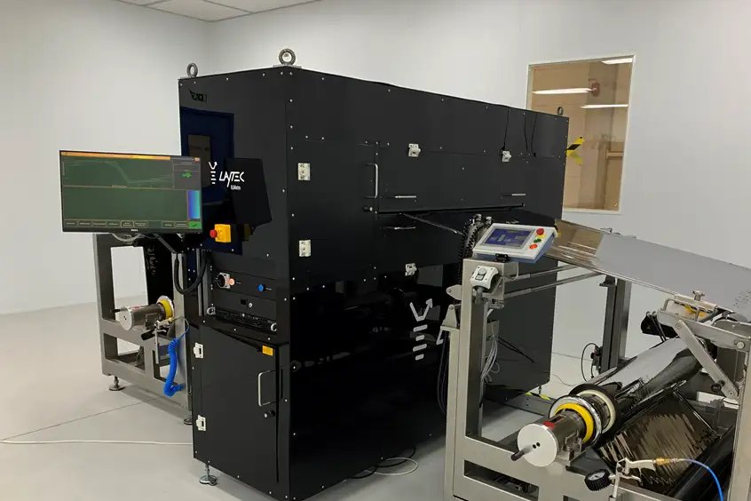
By LayTec GmbH
Combines reflectance, transmittance and Eddy-current measurements for determining properties such as reflectivity, transmission layer thickness and sheet resistance. Additionally, ILMetro R2R is controlling the winding motion enabling fully automated mapping measurements of entire rolls of foil on the km-scale. Alternatively the system can also be integrated into further R2R configurations for measurements on the moving foil. For R&D or additional quality assurance purposes the system also comprises a separate compartment for hand-loaded small-scale samples. With this new product, LayTec successfully enters the market for automated inspection and mapping systems for R2R foil processing.
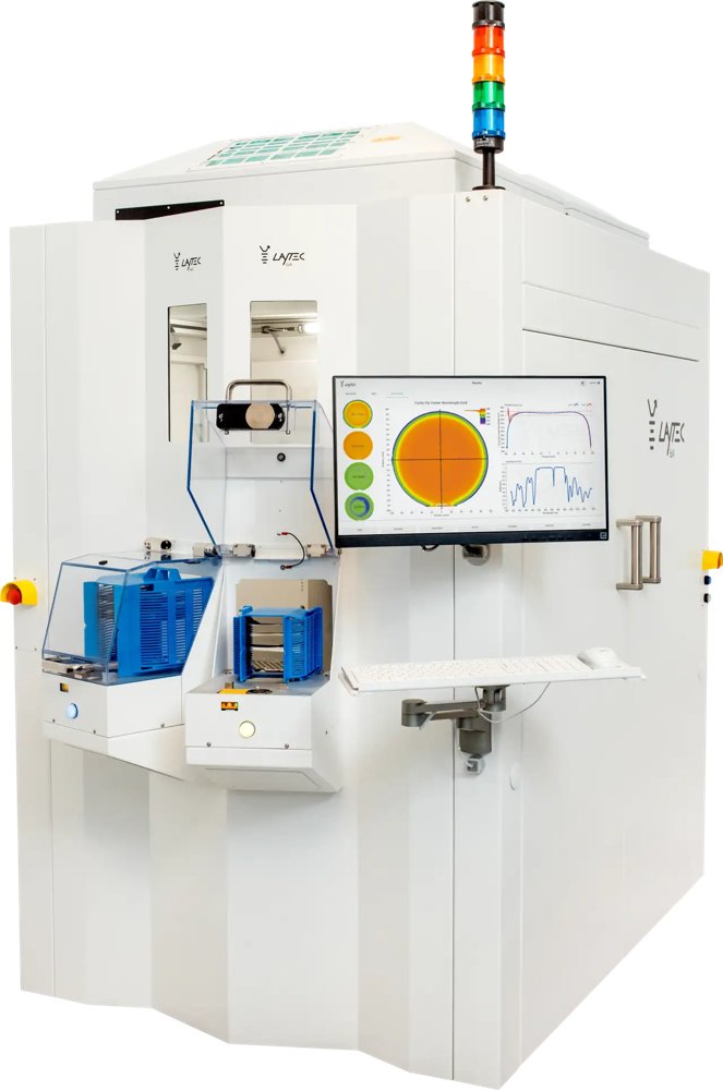
Comprehensive 2D optical wafer mapping for advanced compound semiconductor manufacturing. EpiX® mapping stations provide fast, non-contact 2D measurement of critical optical wafer properties. By combining white light reflectance, photoluminescence and wafer bow mapping in one platform, EpiX® delivers the spatial insight needed to qualify complex epi-stacks and keep high-volume lines in control. What is EpiX®? EpiX® is LayTec’s modular wafer mapping station for ex-situ optical characterization of compound semiconductor and related wafers. An XY mapping stage is combined with UV–VIS–NIR spectroscopic reflectance and photoluminescence metrology, enabling dense 2D maps of thickness, composition and luminescence parameters across the full wafer – all by non-contact optical measurements. Optimized mechanics, optics and signal processing result in: - Very high absolute accuracy - Excellent signal-to-noise ratio - Superior 2D measurement uniformity across the wafer - Short measurement times suitable for production The high spectral quality enables advanced analyses such as multi-layer fits, e.g., for GaN HEMT wafers, multiple-peak analysis, precise composition measurements and detailed VCSEL stop-band and cavity-dip evaluations. Key benefits at a glance: - Full-wafer visibility – 2D maps of thickness, composition, bow and luminescence parameters across the entire wafer surface - Higher yield and tighter specs – quickly identify non-uniformities, drifts and excursions before they impact device performance - Production-ready throughput – cassette-to-cassette automation (EpiX® C2C) with optimized recipes for high-volume lines - R&D flexibility – manual configurations for research and pilot lines using the same analysis methods as production - Robust, upgradeable platform – modular hardware and software to adapt to new materials, device concepts and wavelength ranges Fields of application EpiX® is used across a wide range of compound semiconductor and optoelectronic processes, including: GaN power electronics - 2D maps of AlGaN barrier composition and thickness in D-Mode and E-Mode GaN-on-Si power device wafers - Measurement of p-GaN thickness and total stack thickness - Optional mapping of wafer bow and yellow PL for additional process insight InP-based optoelectronics - PL mapping in the NIR range for InP-based laser and detector structures - 2D profiles of peak wavelength, intensity and other luminescence parameters linked to composition and layer quality LEDs, µLEDs and laser structures - Combined WLR and PL mapping for LED and laser wafers - 2D maps of peak, centroid and dominant wavelength, intensity and spectral width - Thickness and total stack analysis where reflectance is configured VCSEL wafers - Absolute reflectance mapping for stop-band (SB) and cavity-dip (CD) analysis - Extraction of SB center wavelength, width and amplitude - Detailed CD center wavelength, width and area for die-level pass/fail classification Custom materials and layer stacks - Configurable spectral range (UV to NIR) and laser wavelengths - Support for a wide range of epi-stacks and layer systems, including custom stacks in R&D and pilot lines Product features - Fully automated wafer mapper with wafer handler and cassette-to-cassette feature - Combined white light reflectance and photoluminescence mapping - Wavelength range and PL-laser wavelength customizable - PL laser controller with up to 4 wavelengths - Automated yield analysis - Further metrology methods and components upon request - Integrated analysis features such as: - VCSEL stop band and Cavity dop position/width/height - AlGaN barrier composition and thickness of E-Mode and D-Mode GaN-on-Si power device wafers - Single layer, multiple layer and substrate thickness and composition fits - Multiple-peak analysis - Total thickness variation C2C features: - Wafer size 3” – 200mm (300mm option available) - Open cassette, SMIF and FOUP load ports - Pre-aligner - Wafer ID reader - Fan-Filter-Units Comprehensive optical wafer mapping - combined white light reflectance, photoluminescence and bow EpiX® mapping stations can be equipped with: - White light reflectance (WLR) for spectral analysis of layer thicknesses and compositions as well as total stack thicknesses. - Photoluminescence (PL) for bandgap-related parameters such as peak wavelength, composition, intensity and line shape. - Wafer bow metrology for curvature and strain monitoring The spectral range and PL laser wavelength can be configured to your material system, with options for multiple laser wavelengths and extended UV or NIR ranges. This allows EpiX® to be tuned for GaN power, InP optoelectronics, LEDs/µLEDs, VCSELs and many other applications. Optimized for production and R&D EpiX® C2C – high-throughput cassette-to-cassette mapping For industrial production lines, the fully automated EpiX® C2C configuration offers: - Cassette-to-cassette wafer handling for common wafer sizes - Support for open cassette, SMIF and FOUP load ports - Pre-aligner and wafer-ID reader for robust automation - Fan-filter units and cleanroom-compatible design - High-throughput mapping recipes with dense sampling (tens of thousands of spectra per wafer) EpiX® C2C is ideal for routine process qualification, SPC and release of epi-wafers in VCSEL, laser, LED/µLED and GaN-on-Si power lines. Manual EpiX® mapping stations – flexibility for labs The manual EpiX® configurations provide the same optical performance and analysis capabilities in a more flexible setup for: - Universities and research institutes - Pilot and development lines - Process and device R&D teams This makes it easy to transfer recipes and evaluation methods from development to production. Integrated software and automated data analysis EpiX® integrates data acquisition and analysis in a single software environment: - Automated fitting of single-layer, multi-layer and substrate thickness - Determination of composition and other derived parameters - Multiple-peak and DBR/VCSEL analysis routines - Wafer-level and die-level statistics, including pass/fail maps - Recipe-based measurement and evaluation for reproducible results This enables fast routine use on the fab floor while still providing deep analysis capabilities for engineering teams. Modular Design The basic design feature of EpiX® mapping stations is modularity and customizability in hardware and software. This is key for industrial customers introducing new processes and requiring extended measurement capabilities as well as academic customers regularly adjusting their research projects to new materials and latest nano-science concepts. Hence, EpiX is designed as a long-lasting workhorse with multiple upgrade options: more optical heads (wafer bow, reflectance-anisotropy, sheet-resistance, wafer thickness, optical transmission), extended wavelength range, software interfaces (e.g. for user-owned spectral analysis libraries) and for using in-situ data measured during epitaxy in center of wafer as starting point for post-epi 2D mapping analysis.
CATEGORY
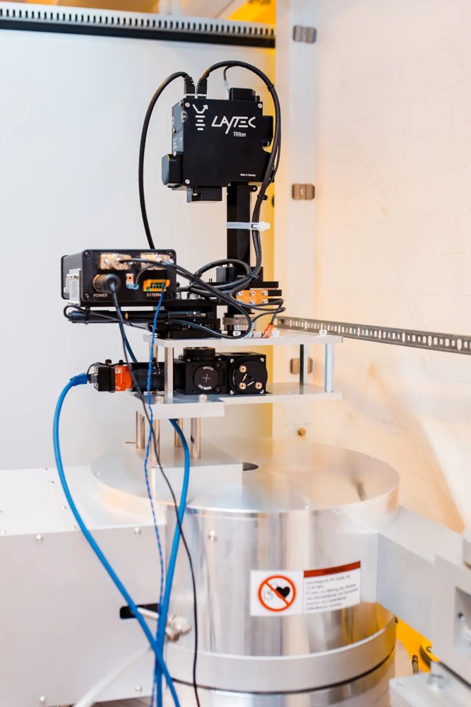
Automated endpoint detection for plasma etching with multi‑wavelength in‑situ reflectometry. As device architectures become thinner and more complex, time-based etching is no longer reliable. Etch rate can drift within a run and across wafers due to chamber conditions, wafer properties, and process history. TRIton® is LayTec’s in‑situ reflectometry solution that brings real-time etch depth control and fully automated endpoint detection (EPD) to plasma etching processes. Key takeaway: TRIton® measures the reflectance transient at three optimized wavelengths during etching and uses this data to track etch progress, detect interfaces, calculate remaining thickness, and stop the process at the right moment – even when etch rate varies. What is TRIton®? TRIton® is an in‑situ optical metrology system for dry etching (e.g., ICP‑RIE, RIE, and ALE) designed to provide robust endpoint detection down to nanometer-level precision on advanced semiconductor layer stacks. It is especially useful when you must stop: - within a layer (residual thickness target), - at a thin-film interface (layer-to-layer transition), - or after a defined etch depth (absolute depth target). For setup and operation, TRIton® supports camera-based spot positioning (useful for patterned wafers and repeatable placement on the correct feature). Why multi‑wavelength reflectometry (and why single-wavelength is often not enough) Many commercial endpoint systems rely on a single wavelength. In complex stacks, this creates a trade‑off: - Long wavelengths penetrate deeper and can show Fabry‑Pérot oscillations (FPOs) useful for depth tracking – but they may miss thin interfaces. - Short wavelengths can be highly sensitive to interfaces – but may be too strongly absorbed for reliable depth tracking across thicker regions. TRIton® solves this by measuring three wavelengths simultaneously, selected based on the optical properties of your material system (wavelength selection is configurable roughly across the UV-NIR range). This enables etch rate extraction and interface detection at the same time, without compromising one for the other. Examples of wavelength sets used in published use cases include: - GaN/AlGaN: near‑UV + UV combinations to combine FPO tracking and sensitive interface detection - GaAs/AlGaAs: visible + NIR combination for rate + interface identification in thick stacks - InP heterostructures: shorter wavelengths for interface sensitivity plus a longer wavelength for depth control. Fields of application - Monitoring of etch processes - Endpoint detection for nitrides, arsenides, and phosphides - Inductively coupled plasma (ICP) etching, reactive ion etching (RIE) & atomic layer etch processes (ALE) - GaN power devices (HFET recess etch) - InP-based lasers (heterostructures & MQW proximity) - GaAs laser diodes - and many other materials Product features - Within layer EPD for various materials and process classes - Automatic and reproducible endpoint detection for plasma etching - Low latency real time endpoint control - Down to sub-nm endpoint resolution - Camera-based point and click measurement spot positioning - UV to NIR measurement wavelength selection - Multiple measurement zones - Layer interface detection - Etch depth control - Remaining layer thickness control - Immune to etch-rate variation - Graphical endpoint recipe development - Endpoint interface for automated etch stop - Remote control interface for full integration into etcher Features What TRIton® can control in real time Depending on your stack, etch chemistry, and recipe design, TRIton® supports real-time monitoring and control of: - Etch depth progress (via reflectance features and/or FPO analysis) - Etch rate and etch rate drift during the run (enabling adaptive control vs fixed etch time) - Interface detection (via slope/contrast changes at sensitive wavelengths) - Remaining thickness targeting for within-layer stops (critical for recess and gate structures) - Optional: system health / chamber conditioning insight by tracking run-to-run etch behavior and correlating optical/plasma signals TRIton® in the LayTec Connected Metrology® ecosystem (“from epi to etch”) TRIton® becomes even more powerful when paired with upstream and downstream LayTec metrology: - Use EpiCurve® TT / EpiTT during epitaxy to capture accurate growth thickness/composition data, - Use EpiX® for ex‑situ 2D wafer mapping (uniformity, PL/reflectance), - Use TRIton® in plasma etch for in‑situ thickness tracking and endpointing. This “from epi to etch” approach supports tighter specs and better die-level understanding in advanced front-end flows.
CATEGORY
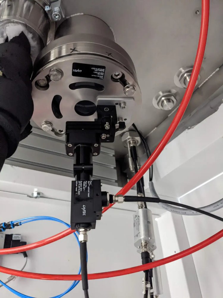
LayTec’s spectral in-situ monitoring tool for various compound semiconductors such as perovskites and CIGS. Perovskites and similar materials are manufactured by a variety of processes such as thermal evaporation in vacuum or spin coating. Typically, in the latter case, subsequent thermal annealing under inert gas atmosphere is also applied. Similarly, CIGS growth is a complex multi-step process based on co-evaporation or sputtering and selenization. InspiRe is well-suited for spectral monitoring like complex and rapid growth and phase formation processes due to its rapid acquisition rates in the millisecond range. Fields of application - Monitoring of rapidly changing liquid solution films during spin coating or evaporation - Providing real-time reflectance information during perovskite annealing revealing phase or surface transformations including visualization of growth rates, surface roughness and absorption edges - Real time growth rate and film thickness measurements - Real-time visualization of absorption edge and reaction kinetics - Optimization of coating and annealing times for other complex and/or multi-component materials - Monitoring of co-evaporation or sputtering processes for CIGS or TCO materials in vacuum chambers Product features - Spectral reflectance monitoring in the VIS or NIR range - Sampling times of down to 0.5 ms - Various monitoring modes can be selected: 2D spectrogram, transients of chosen wavelengths, spectral analysis at selected process times - Can be combined with spectral and / or time-resolved in-situ photoluminescence metrology systems PearL and t-PearL for room temperature processes. - Real-time growth-rate/thickness measurements by various algorithms - Fingerprint run-to-run analysis based on 2D spectrograms Features - InspiRe is available for various wavelength ranges in the VIS and NIR depending on materials and process requirements. - Multi-head versions of InspiRe are available on request. - PearL and t-PearL photoluminescence metrology system can be combined with InspiRe for room-temperature processes. In these cases all metrology methods can usually be combined in one shared measurement head For high-temperature (T400°C), the InspiRe metrology system can be combined with EpiTT and or EpiCurve TT metrology systems and act as their spectral reflectance extension as in the EpiTT VCSEL system.
CATEGORY
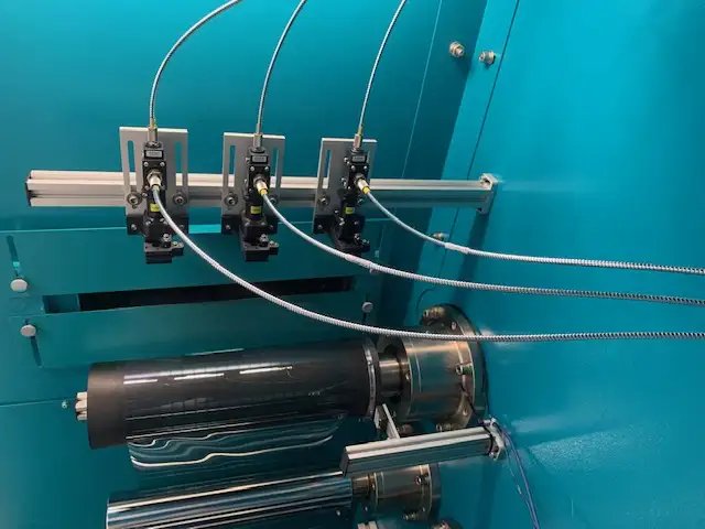
In-line monitoring multi-layer thin-film structures in large area processes by means of spectral reflectance LayTec's Flames is a multi-head optical metrology system for in-line monitoring of multi-layer thin-film structures in large area coating processes. It measures multiple traces of layer thickness, reflectance, and transmittance for assessing sample uniformity directly after the deposition in in-line configuration with thickness resolutions down to less than 1 nm. Typical applications are functional layers in thin film photovoltaics, display industries, foil coating (roll-to-roll), and glass coating in general. Flames is suitable for nearly any thin-film production line. With its contact-free optical approach it measures close to the process and allows closed-loop control of layer deposition and etching. With LayTec Flames you get homogeneity information of the layers at the tact rate of your line, directly after processing, complete with statistical analysis. You can apply quality thresholds and alarms for fast reaction of operators Fields of application - Reflectance and transmittance measurements for functional glasses and foils - Layer thickness measurements for functional glasses and foils - Integration into production lines for sheet-to-sheet (S2S) or roll-to-roll (R2R) manufacturing - Characterization of various layers such as: - antireflective or IR-reflective coatings - CIGS, perovskites, CdTe, CdSe, CdS or organic photovoltaic materials - Electrochromic glasses - Displays and OLEDs - Food packaging foils - Decorative foils Product features - Reflectance, transmittance monitoring at up to seven traces - Layer thickness can be calculated based on sophisticated optical models - Customized optical mounts to meet the requirements of your automation system - PV-line software integration via Profibus, Ethernet, TCP/IP or other protocols for automated operation - Like PearL and t-PearL, Flames can be a component of ILMetro stations Features - Fully automated in-line monitoring of thin film thickness during production - Up to seven traces along the substrate can be measured - Available for VIS, NIR and combined spectral range - Further information about transmission, color, roughness and band gap can be deduced - Eddy-current measurements can be added on demand
CATEGORY
