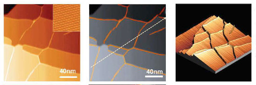
Graphene has generally been described as a two-dimensional structure—a single sheet of carbon atoms arranged in a regular structure—but the reality is not so simple. In reality, graphene can form wrinkles which make the structure more complicated, potentially being applied to device systems. The graphene can also interact with the substrate upon which it is laid, adding further complexity.
In research published in Nature Communications, RIKEN scientists have now discovered that wrinkles in graphene can restrict the motion of electrons to one dimension, forming a junction-like structure that changes from zero-gap conductor to semiconductor back to zero-gap conductor. Moreover, they have used the tip of a scanning tunneling microscope to manipulate the formation of wrinkles, opening the way to the construction of graphene semiconductors not through chemical means—by adding other elements—but by manipulating the carbon structure itself in a form of “graphene engineering.”
The discovery began when the group was experimenting with creating graphene films using chemical vapor deposition, which is considered the most reliable method. They were working to form graphene on a nickel substrate, but the success of this method depends heavily on the temperature and cooling speed.
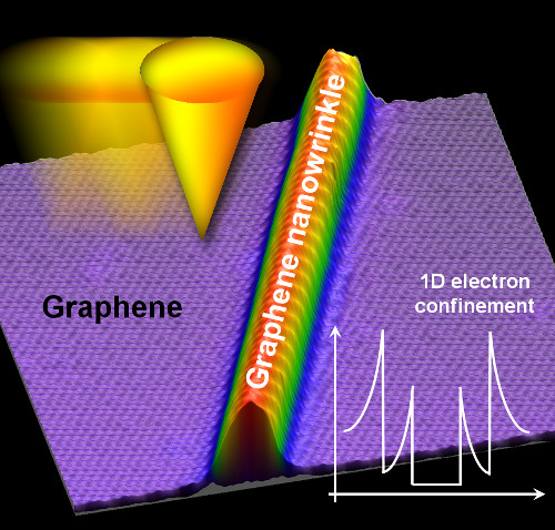
According to Hyunseob Lim, the first author of the paper, “We were attempting to grow graphene on a single crystalline nickel substrate, but in many cases we ended up creating a compound of nickel and carbon, Ni2C, rather than graphene. In order to resolve the problem, we tried quickly cooling the sample after the dosing with acetylene, and during that process we accidentally found small nanowrinkles, just five nanometers wide, in the sample.”
They were able to image these tiny wrinkles using scanning tunneling microscopy, and discovered that there were band gap openings within them, indicating that the wrinkles could act as semiconductors. Normally electrons and electron holes flow freely through a conductor without a band gap, but when it is a semiconductor there are band gaps between the permitted electron states, and the electrons can only pass through these gaps under certain conditions. This indicates that the graphene could, depending on the wrinkles, become a semiconductor. Initially they considered two possibilities for the emergence of this band gap. One is that the mechanical strain could cause a magnetic phenomenon, but they ruled this out, and concluded that the phenomenon was caused by the confinement of electrons in a single dimension due to “quantum confinement.”
According to Yousoo Kim, head of the Surface and Interface Science Laboratory, who led the team, “Up until now, efforts to manipulate the electronic properties of graphene have principally been done through chemical means, but the downside of this is that it can lead to degraded electronic properties due to chemical defects. Here we have shown that the electronic properties can be manipulated merely by changing the shape of the carbon structure. It will be exciting to see if this could lead to ways to find new uses for graphene.”
RIKEN
#Graphene #Nanomaterials #Semiconductors
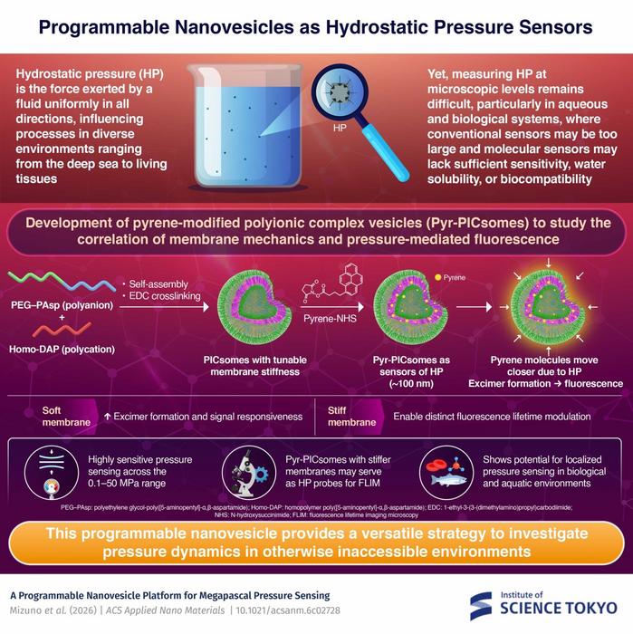
Pyrene-modified polyionic complex vesicles, or Pyr-PICsomes, convert hydrostatic pressure into measurable fluorescence. Crosslinking density tunes membrane stiffness, which governs sensing behavior: soft vesicles give strong excimer-to-monomer ratio changes from 0.1 to 50 MPa, while stiff membranes respond through fluorescence lifetime, suiting lifetime imaging.
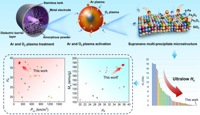
Ar/O₂ plasma treatment generates supranano α-Fe, Fe₃O₄, SiO₂ and Fe₂O₃ precipitates just 0.8–2.5 nm across amorphous powder surfaces, creating nucleation sites that ease magnetic-moment reversal. The resulting soft magnetic composite combines 0.13 Oe coercivity, 37.3 permeability, 185 emu g⁻¹ saturation magnetization and 191.18 kW m⁻³ core loss at 1 MHz and 20 mT. The surface route avoids bulk composition changes, aiding scale-up for high-frequency inductors and power chokes.
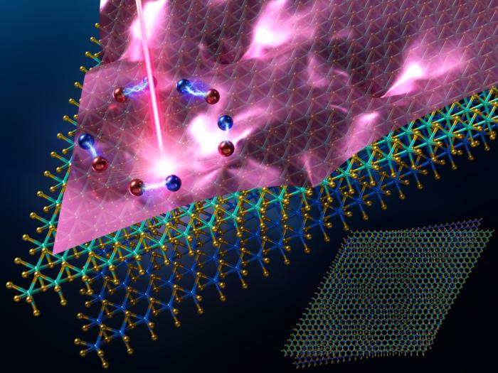
Researchers at MANA have introduced a theoretical framework that extracts hidden disorder from complex photoluminescence spectra in twisted MoSe2/WSe2 moiré heterostructures, bypassing unreliable peak-by-peak analysis. By tracking how simple descriptors like peak and average energy vary spatially, the work reveals a hierarchy of disorder, from micrometer-scale background variations to localized exciton-trapping defects.