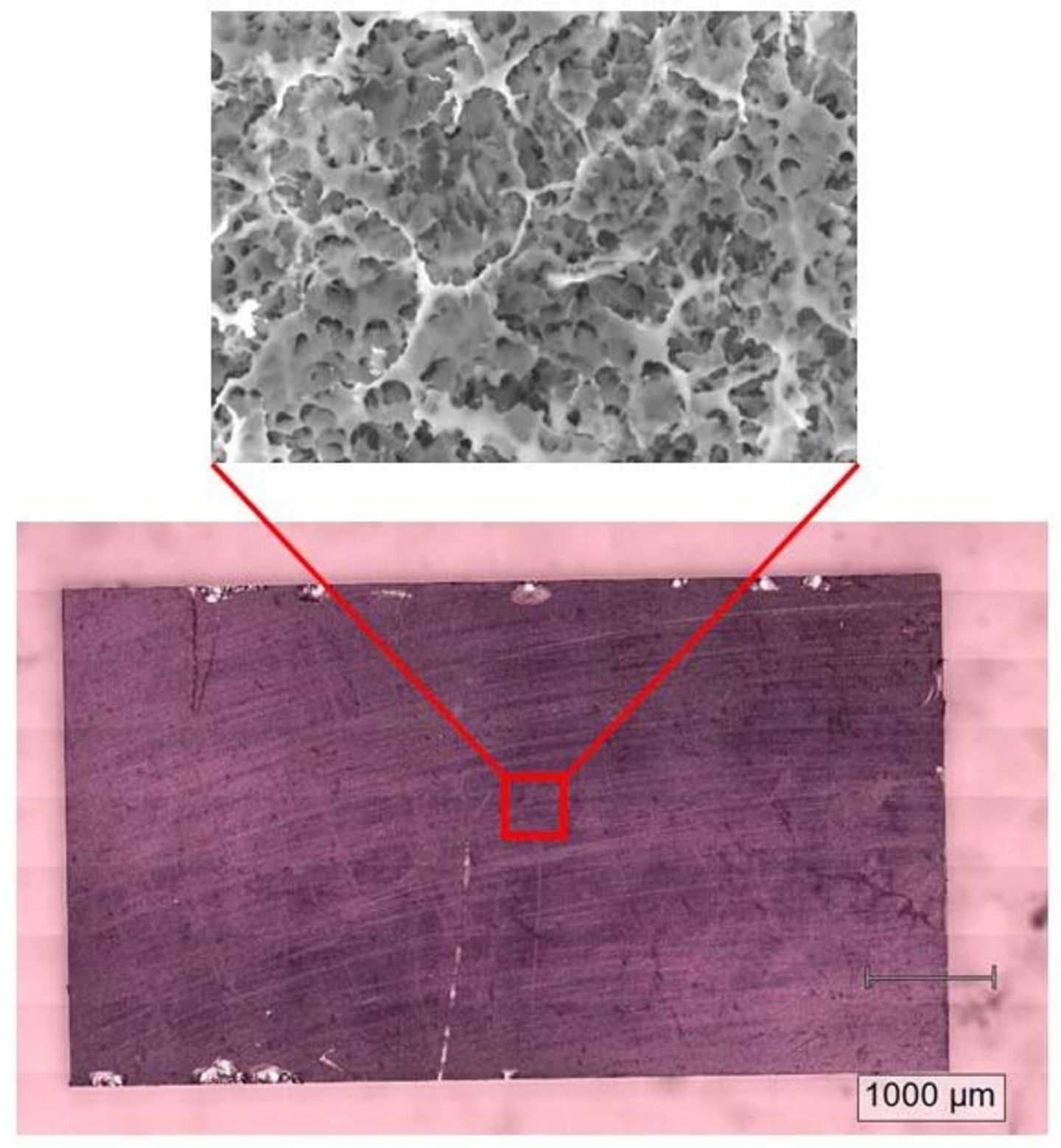
The carbon material graphene has no well-defined thickness, it merely consists of one single layer of atoms. It is therefore often referred to as a "two-dimensional material". Trying to make a three-dimensional structure out of it may sound contradictory at first, but it is an important goal: if the properties of the graphene layer are to be exploited best, then as much active surface area as possible must be integrated within a limited volume.
The best way to achieve this goal is to produce graphene on complex branched nanostructures. This is exactly what a cooperation between CNR Nano in Pisa, TU Wien (Vienna) and the University of Antwerp has now achieved. This could help, for example, to increase the storage capability per volume for hydrogen or to build chemical sensors with higher sensitivity.
From solid to porous
In Prof. Ulrich Schmid’s group (Institute for Sensor and Actuator Systems, TU Wien), research has been conducted for years on how to transform solid materials such as silicon carbide into extremely fine, porous structures in a precisely controlled way. "If you can control the porosity, then many different material properties can be influenced as a result," explains Georg Pfusterschmied, one of the authors of the current paper.
The technological procedures required to achieve this goal are challenging: "It is an electrochemical process that consists of several steps," says Markus Leitgeb, a chemist who also works in Ulrich Schmid's research group at TU Wien. "We work with very specific etching solutions, and apply tailored electric current characteristics in combination with UV irradiation." This allows to etch tiny holes and channels into certain materials.
Because of this expertise in the realization of porous structures, Stefan Heun's team from the Nanoscience Institute of the Italian National Research Council CNR turned to their colleagues at TU Wien. The Pisa team was looking for a method to produce graphene surfaces in branched nanostructures to enable larger graphene surface areas. And the technology developed at TU Wien is perfectly suited for this task.
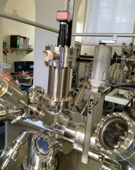
"The starting material is silicon carbide - a crystal of silicon and carbon," says Stefano Veronesi who performed the graphene growth at CNR Nano in Pisa. "If you heat this material, the silicon evaporates, the carbon remains and if you do it right, it can form a graphene layer on the surface."
An electrochemical etching process was therefore developed at TU Wien that turns solid silicon carbide into the desired porous nanostructure. About 42 % of the volume is removed in this process. The remaining nanostructure was then heated in high vacuum in Pisa so that graphene formed on the surface. The result was then examined in detail in Antwerp. This revealed the success of the new process: indeed, a large number of graphene flakes form on the intricately shaped surface of the 3D nanostructure.
A lot of surface area in a compact form
"This allows us to use the advantages of graphene much more effectively," says Ulrich Schmid. "The original motivation for the research project was to store hydrogen: you can temporarily store hydrogen atoms on graphene surfaces and then use them for various processes. The larger the surface, the larger the amount of hydrogen you can store." But there are also many other ideas for using such 3D graphene structures. A large surface area is also a decisive advantage in chemical sensors, which, for example, can be used to detect rare substances in gases.
Reference
3D arrangement of epitaxial graphene conformally grown on porousified crystalline SiC
Stefano Veronesi, Georg Pfusterschmied, Filippo Fabbri, Markus Leitgeb, Omer Arif, Daniel Arenas Esteban, Sara Bals, Ulrich Schmid, Stefan Heun
https://www.sciencedirect.com/science/article/abs/pii/S000862232101201X?via%3Dihub
