
Researchers from the Institute for Photovoltaics at the University of Stuttgart, with collaborators from Forschungszentrum Jülich, INL Braga and AIKO Europe, have shown that an approximately 3 nm atomic-layer-deposited aluminium oxide (AlOx) buffer can protect perovskite-silicon tandem solar cells during indium tin oxide (ITO) sputtering. The work was carried out on an integrated inert-atmosphere processing platform supplied by the Kurt J. Lesker Company.
Thermal ALD was used to deposit AlOx directly onto the C60 electron-transport layer before ITO deposition by pulsed-DC magnetron sputtering. The optimum AlOx thickness was approximately 3 nm, corresponding to 38 ALD cycles. The film formed a dense, conformal coating that protected the device stack during sputtering.
In the reported comparison, thin SnOx films more frequently showed incomplete coverage and pinhole formation. Within the device architecture and process conditions investigated, the approximately 3 nm AlOx layer provided effective sputter protection compared with an approximately 20 nm SnOx buffer layer, a reduction of approximately 85% in nominal buffer-layer thickness.
Semi-transparent perovskite solar cells with the ultrathin AlOx protection layer reached power-conversion efficiencies above 17%. Monolithic perovskite-silicon tandem devices exceeded 26%, with independent reporting citing a tandem efficiency of approximately 26.9%. In an initial thermal-stress test, devices were held at 85 °C in dry air for four hours; AlOx-buffered devices showed approximately 1.6% relative efficiency loss, against approximately 8.0% for SnOx-buffered devices.
The ultrathin AlOx layers were deposited using a glovebox-integrated KJLC ALD150LE before transfer to sputtering. The platform connects solution processing, thermal evaporation, ALD and sputtering through glovebox environments, allowing sensitive samples to move between process stages without exposure to ambient air. The researchers state that longer-duration reliability studies would be needed to assess commercial lifetime.
Source: Kurt J. Lesker Co. Ltd. news

Researchers at Imperial College London and the University of Exeter tracked how a 310-nm indium tin oxide film switches its optical response under intense femtosecond pulses, near its epsilon-near-zero wavelength. Transmission rose by up to 280 percent while reflection fell by as much as 74 percent, then saturated as electrons below the Fermi level were depleted. A microscopic model fits the shift and predicts switching within a few femtoseconds.
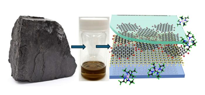
Researchers at the University of Illinois Urbana-Champaign and NETL have shown that carbon nanodots derived from bituminous coal can serve as an atomic-scale interfacial binder for integrating high-κ dielectrics with 2D semiconductors such as molybdenum disulfide.

Purdue University researchers have unveiled three ThermiQuant molecular diagnostics instruments built on a paper-based biosensor that uses loop-mediated isothermal amplification to detect pathogen DNA and RNA through color change. The devices span high-throughput lab scanning, portable benchtop testing for clinics and farms, and a solid-state version with dual-sided indium tin oxide heating that holds stable reaction temperatures from 4 to 50 degrees Celsius.
This week in nanotech
$751.8M raised
6 funding rounds · 37 deals tracked
New products
 Ti-WCMBN Nanomaterialia Featured
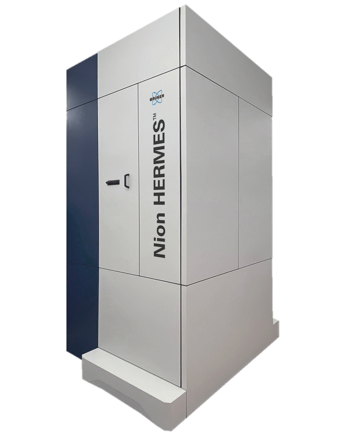 Nion-compatible In Situ STEM Holders for Electrical BiasingHummingbird Scientific Featured
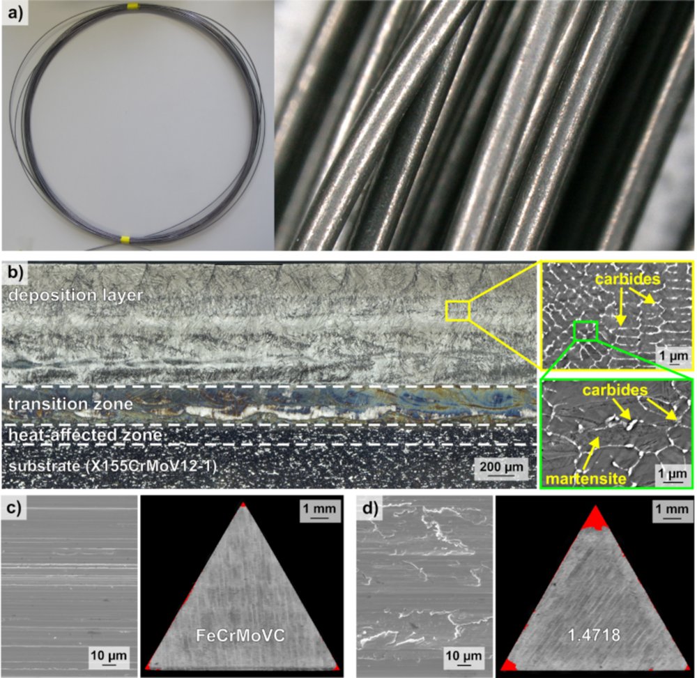 Fe85Cr4Mo8V2C1 wire filler materialLeibniz Institute for Solid State and Materials Research Dresden - IFW Dresden
Market insights
Last 30 days: Quantum Technologies drew the most money: $3.18B.
Money raised per month
Behind the deal
Who invested in Vertical Semiconductor’s $73M Grant?
See the investors with Insights Pro →