Los Angeles, 21 October 2026. California Nanotechnologies Corp. has signed an amendment to its existing Santa Ana facility lease to support its manufacturing capacity expansion, the company announced on October 21, 2026.
The amendment adds 15,500 square feet of adjacent space, an approximate 80% increase to the company's existing 19,500 square feet footprint. It also provides access to increased electrical current capacity to power its core technologies and other equipment.
"This lease amendment is timely as we look to expand our production capacity for customers," said Eric Eyerman, CEO. "Earlier this month, we announced our largest single purchase order and a new development agreement with a Fortune 100 multinational, which will require resources to ensure we can successfully deliver. The larger floor and office space, loading docks, electrical capacity, and storage are all key logistical components of being able to scale up."
The new lease takes effect on November 1, 2026, and will cost approximately US$22,500 per month. The company said the amendment follows its consolidation of the Cerritos facility into Santa Ana earlier in the fiscal year, which provided approximately US$10,000 per month in savings.
California Nanotechnologies processes metallurgic powders into parts and operates two manufacturing facilities in Greater Los Angeles. Its customers include Fortune 500 companies and startups, with programs in aerospace, renewable energy, defense and semiconductors. The company's capabilities include multiple in-house spark plasma sintering systems, cryogenic mills, mechanical testing and tooling fabrication.
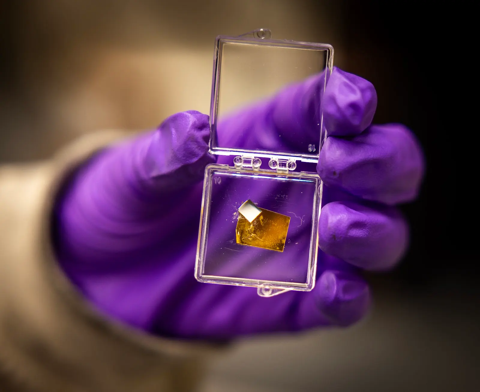
University of Michigan and University of Wisconsin researchers, backed by up to $6M from DARPA, propose an alternative to the transistor that could make computing 100 to 1,000 times faster and more energy efficient. The M3BOLT device pairs ferroelectric PMN-PT with a magnetic iron-gallium alloy, using magnons and sound waves instead of moving electrons as bits. Magnetic states also persist without power, adding memory.
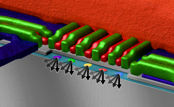
Silicon spin qubits usually lose accuracy when many qubits are driven in parallel, a barrier to scalable quantum processors. Writing in Nature Physics, RIKEN researchers traced the main error source to AC Stark shifts from shared microwave control signals. Their pairwise phase calibration protocol restored gate fidelities above 99.99% for up to three simultaneous qubits, and about 99.9% across all five, near fault-tolerant requirements.
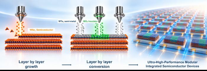
Researchers at the Institute for Basic Science converted a single tungsten diselenide crystal into a working transistor by selectively oxidizing and reacting its top atomic layers. The resulting tungsten oxide served as a sub-nanometer gate dielectric, while tungsten ditelluride contacts cut the charge injection barrier to about a third of that seen with platinum.
This week in nanotech
$91M raised
8 funding rounds · 55 deals tracked
New products
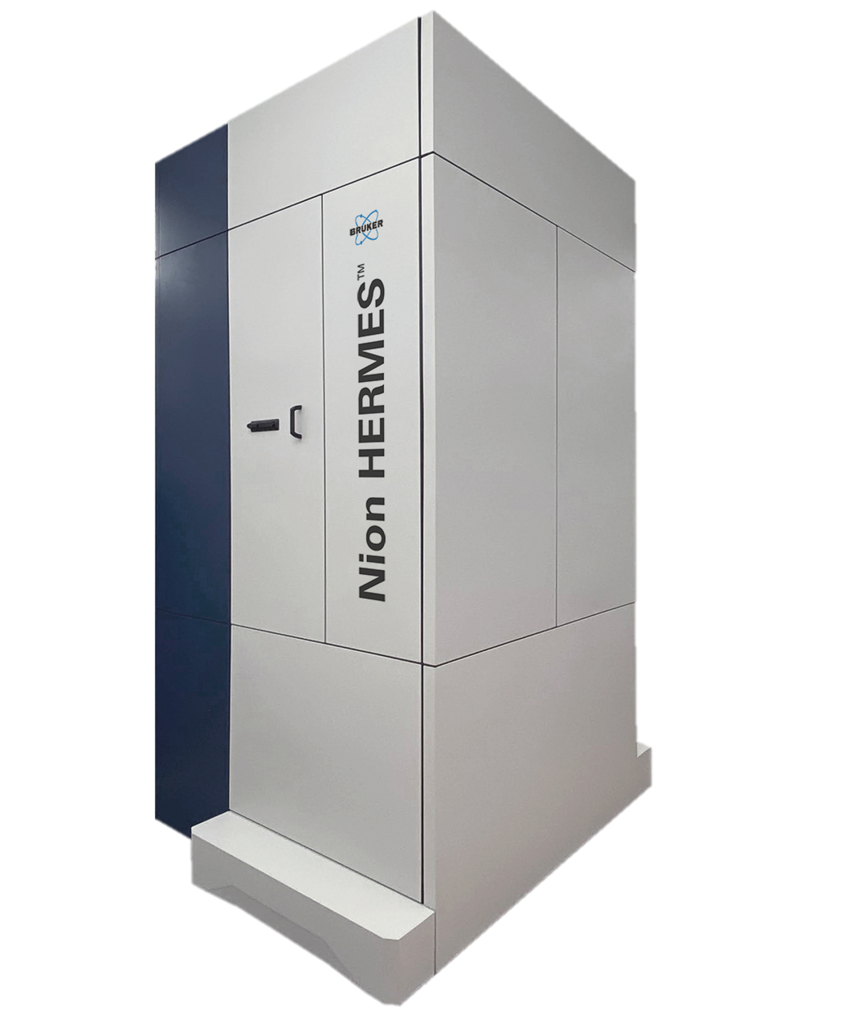 Nion-compatible In Situ STEM Holders for Electrical BiasingHummingbird Scientific Featured
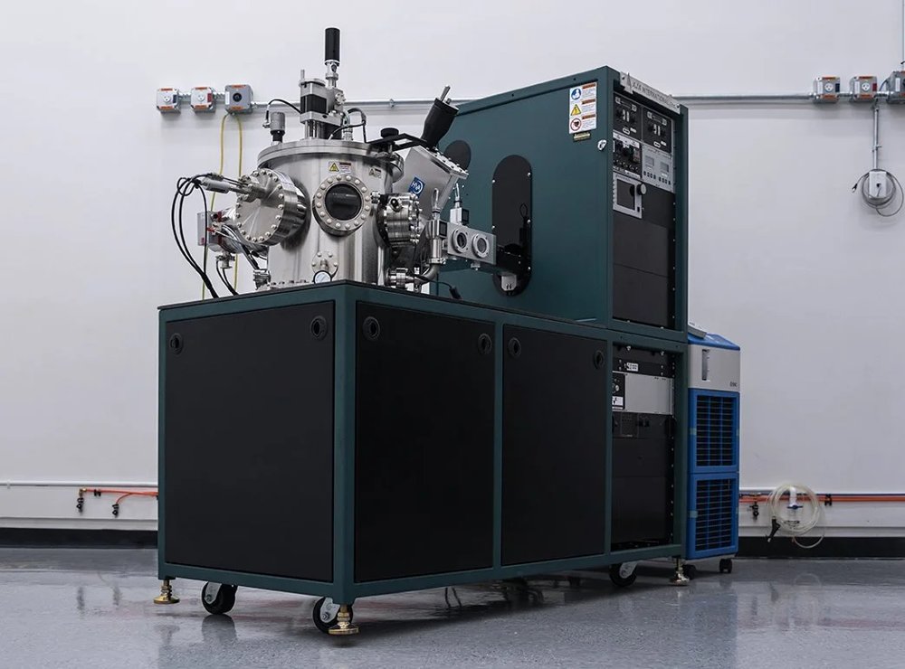 Orion Sputtering Deposition SystemsAJA International Featured
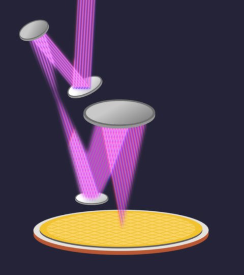 Aether®Lam Research
Market insights
Last 30 days: Quantum Technologies drew the most money: $3.17B.
Money raised per month
Behind the deal
Who led Xanadu Quantum Technologies Limited’s $10M Grant?
See the investors with Insights Pro →