Compact photonic chip enables three-dimensional OCT inspection for industrial samples
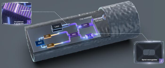
Researchers at Shanghai Jiao Tong University have developed a 0.36-mm² photonic chip designed for industrial swept-source optical coherence tomography (SS-OCT). As reported in PhotoniX Synergy, this compact system enables high-precision 3D imaging and contactless measurement, with a ball-lens fiber probe that facilitates inspection within confined spaces.
While OCT is a well-established medical imaging modality, it is increasingly gaining traction in industrial sectors. To achieve widespread adoption, however, systems must become more cost-effective and robust. Photonic integrated circuits (PICs) offer a promising solution for developing compact, low-cost, and maintenance-free OCT engines. Despite this potential, mass-producing robust PIC-based OCT systems remains challenging, particularly regarding material selection for foundry-based fabrication and the integration of flexible sample arms.
To address these hurdles, the research team integrated low-loss silicon nitride interferometers with germanium photodiodes on a commercially fabricated silicon-based chip. An interlayer coupling structure facilitates light transfer between the silicon nitride and silicon waveguides with a coupling loss of less than 0.15 dB. This design consolidates key optical components into a 0.9 × 0.4 mm footprint while maintaining the flexibility to connect various sample arms.
“Our aim was to create a compact OCT module adaptable to practical industrial inspections,” said Xingchen Ji, associate professor at Shanghai Jiao Tong University and corresponding author. “Integrating the interferometer and photodetectors on-chip reduces the number of discrete optical components, while the fiber-connected sample arm significantly expands the system’s operational range.”
In experimental testing, the system achieved 87-dB sensitivity and a 3.42-mm sensitivity roll-off range. It successfully resolved internal structures within a smartphone camera. Furthermore, its contactless thickness measurements of a silica wafer showed an absolute error of less than 2 µm compared to contact-based methods, while measurements of soft SU-8 photoresist blocks yielded a relative error of under 0.12%.
By connecting an angle-polished, 450-µm-diameter ball-lens fiber probe, the researchers demonstrated the system’s ability to capture 3D images of threads inside a metal optical post and internal layers within a rolled plastic tape.
“Contactless measurement is invaluable when physical contact could deform a soft surface,” noted Hang Su, first author and doctoral student at Shanghai Jiao Tong University. “The fiber probe also allows us to examine structures that are inaccessible to conventional microscopes. This plug-and-play OCT module paves the way for the next generation of chip-scale OCT engines.”
Reference Robust and plug-and-play chip-based swept-source optical coherence tomography for industrial applications
Hang Su, Shuo Wang, Jianing Mao, Chunxue Wang, Mengyuan Wang, Jie Zhang, Yuye Ling, Xingchen Ji, and Yikai Su
Chinese Society for Optical Engineering