
Osaka, Japan – A research team led by the University of Osaka has directly observed an unusual heavy-fermion state forming at the boundary between a one-atom-thick material and a metal for the first time. Such states are closely linked to exotic quantum phenomena, including unconventional superconductivity, and the finding opens new possibilities for designing quantum materials through their interfaces.
The researchers created a high-quality, one-atom-thick layer of ytterbium–copper (YbCu₂) on a copper crystal and examined how electrons behaved across the interface using intense synchrotron light. Their measurements showed that electrons localized in the atomic layer interact with mobile electrons in the underlying copper to form the heavy-fermion state.
The measurements revealed two distinct heavy-fermion states. One was confined mainly to the two-dimensional YbCu₂ layer, while the other extended into the three-dimensional copper substrate. Crucially, the latter arose from hybridization between localized Yb 4f electrons in the atomic layer and mobile conduction electrons in the underlying copper, providing direct evidence of an interfacial heavy-fermion state.
“This achievement was made possible by our continued efforts to create high-quality materials and measure their electronic states as precisely as possible,” says senior author Professor Shin-ichi Kimura. “Our next goal is to engineer and control such heavy-electron states, opening the way to previously unexplored quantum states, including unconventional superconductivity.”
The findings suggest that carefully combining atomic layers and substrates could provide a new approach to designing quantum materials. By precisely controlling interfacial structures, electronic orbitals, and moiré patterns, researchers may be able to create and tune new low-dimensional quantum phenomena that cannot be realized in conventional materials.
Reference
Interfacial heavy fermion formation in a two-dimensional Kondo lattice YbCu2 on Cu(111) substrate
Takuto Nakamura, Hiroki Sugihara, Toshio Miyamachi, Yitong Chen, Kaito Nishihara, Ryo Ichikawa, Hiroka Yamaguchi, Ryu Yukawa, Kiyohisa Tanaka, Yuri Hasegawa, Yoshiyuki Ohtsubo, Fumio Komori, and Shin-ichi Kimura
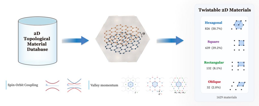
Two new studies catalog nearly 9,000 two-dimensional materials and identify 61 semimetals and 1,568 insulators suited to twistronics, the stacking and rotating of atomically thin layers to engineer narrow electronic bands. The work maps topological electronic structures, predicts promising twisted bilayers such as tin diselenide and hafnium disulfide, and confirms several candidates can be grown in bulk and exfoliated into working devices, giving researchers a systematic route to designer…
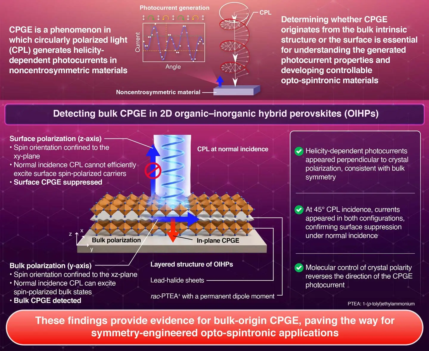
Researchers at Science Tokyo have shown that the circular photogalvanic effect in two-dimensional organic-inorganic hybrid perovskites arises from the crystal bulk rather than its surface. Using circularly polarized light at normal incidence, they found helicity-dependent photocurrents that reversed with light handedness and with crystal polarity in chiral enantiomers. The lead iodide layers provide strong spin-orbit coupling while molecular cations set bulk polarity.
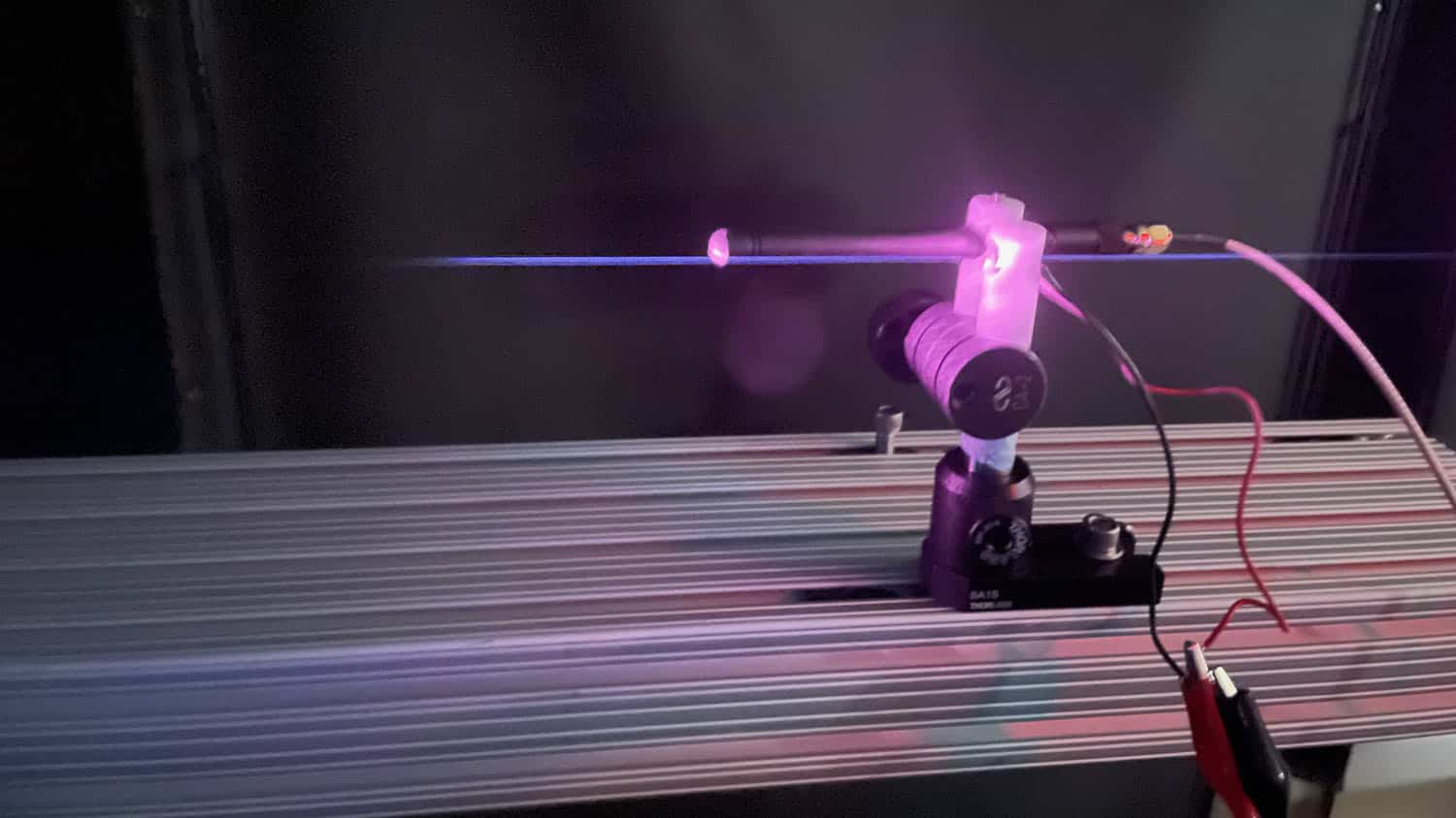
Photo credit: Prya Darshni. Researchers have demonstrated a technique that uses a laser to produce a plasma beam antenna capable of transmitting radio waves. “The plasma beam antenna looks like a lightsaber and is tunable, meaning we should be able to transmit across a broad range of frequencies,” says Prya Darshni, corresponding author of a journal article on the work and a Ph.D. student at North Carolina State University. “And while we have not demonstrated its ability to serve as an...