Max Planck Institute for Chemical Physics of Solids
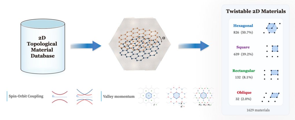
A small twist can fundamentally change the electronic behavior of a material. When two atomically thin crystals are stacked and rotated relative to each other, a larger-scale moiré pattern emerges. This pattern changes how electrons move and interact within the material. This approach, known as twistronics, has already produced striking results. Twisted graphene and transition metal dichalcogenides, for example, have revealed superconductivity and fractional Chern insulators. But research has so far relied on a relatively small number of materials known to work.
Two new studies now greatly expand the range of possible starting points. Rather than focusing on individual materials, the researchers from more than a dozen institutions created a broad map of two-dimensional materials and then systematically searched it for electronic structures particularly suited to twisting. “Every new family of twisted materials gives us a chance to ask a different question about quantum matter. We want to move beyond the few platforms we know and explore the enormous range of physics that other layers and other twists could make possible,” says B. Andrei Bernevig, Professor of Physics at Princeton University and co-author of both studies.
A library of electronic building blocks
The researchers analyzed 8,872 entries from two computational materials databases. To characterize their electronic properties, they extended topological quantum chemistry – a theoretical framework that connects the chemistry and symmetries of a crystal to the topology of its electronic states – to nonmagnetic two-dimensional materials. Crystal symmetries, such as rotations or reflections that leave the atomic arrangement unchanged, provide rules for how electronic states can be organized. Some of these arrangements are topological: their properties cannot change without a fundamental alteration of the electronic structure. Among the 8,872 entries, the researchers identified 4,073 materials with nontrivial topology or an obstructed atomic limit. In the latter, crystal symmetry can constrain the centers of electronic charge to positions away from the atoms, allowing distinctive electronic states to emerge at particular boundaries. The resulting catalog, however, is not limited to topological materials. It records the electronic band structures – the energies available to electrons – of nearly 9,000 two-dimensional systems. In this way, it provides a library of possible building blocks for future layered materials.
Finding materials worth twisting
Two identical layers can be combined into a homobilayer, while two different layers form a heterobilayer. Adding the possibility of rotating these layers relative to each other creates an enormous number of potential combinations. The researchers therefore took the next step: identifying which of these building blocks provide particularly promising starting points for twistronics.
They found 61 semimetals and 1,568 insulators whose electronic structures are suited to twisting while remaining relatively simple to describe theoretically. This matters because twisting suitable materials can produce narrow electronic bands. In such bands, electron motion becomes less dominant and interactions between electrons become particularly influential. These conditions provide fertile ground for phenomena including superconductivity, magnetism and fractional quantum states.
The candidates cover a wide variety of crystal structures, including hexagonal, square, rectangular and oblique lattices. This diversity also opens different possibilities for using twisted materials as quantum simulators – controllable systems that realize models of interacting electrons.Twisted square lattices, for example, could simulate the Hubbard model, which is central to research on high-temperature superconductivity. Rectangular systems could provide access to behavior resembling electrons moving along one-dimensional chains. “A small twist can change the balance between electrons’ motion and their interactions. Different materials give us different ways to tune that balance and look for collective quantum behavior,” explains Hanqi Pi, reseracher at the University of the Basque Country.
Turning theoretical candidates into real crystals
Identifying promising electronic structures is only useful experimentally if the corresponding materials can actually be produced. The researchers therefore calculated selected twisted bilayers and found narrow bands in compounds including tin diselenide and hafnium disulfide. At the same time, experimental teams grew bulk crystals of several candidate materials, including tin diselenide, tin disulfide, gallium telluride and zirconium nitride chloride. Researchers at the Max Planck Institute for Chemical Physics of Solids in Dresden, including Peter Höhn, Vicky Hasse and Claudia Felser, contributed to this experimental work. “A prediction is only useful if the crystal can actually be grown. We can make several of these compounds in bulk, at the size and quality that exfoliation down to single layers requires,” says Claudia Felser, co-author and Director at the Max Planck Institute for Chemical Physics of Solids.
Initial sample preparation confirmed that the grown materials can be exfoliated – peeled down to individual layers. This provides a practical route from materials identified through calculations to atomically thin samples that can be stacked and twisted in experiments. The collaboration has already assembled exfoliated monolayers into working devices, including a twisted homobilayer of hafnium disulfide that was investigated using scanning tunneling microscopy at millikelvin temperatures.
From searching materials to designing quantum systems
Together, the two studies provide a systematic framework for exploring twisted quantum materials. The first catalog supplies a broad set of individual electronic building blocks. The second identifies those with particularly suitable starting conditions for twisting. The next step is to build more devices from these materials and experimentally investigate their collective behavior. Instead of relying on the small number of materials already established in twistronics, researchers can now compare electronic structures and select candidates according to the physical questions they want to investigate. “We would like to take a problem about interacting electrons and ask which crystal, which layers and which twist will let us study it,” Bernevig says. “The exciting part is that an experiment can also show us something we did not know to ask.”
This Article was written with Material by the University of Princeton which we kindly thank for their work.
Reference
2D theoretically twistable material database
Yi Jiang, Urko Petralanda, Hanqi Pi, Grigorii Skorupskii, Qiaoling Xu, Dumitru Călugaru, Haoyu Hu, Jiaze Xie, Rose Albu Mustaf, Peter Höhn, Vicky Haase, Abdelmajid Ouahchi, Soumyajit Samal, Jiacheng Zhu, Dongyang Yang, Zuhan Geng, Garen Avedissian, Yongsong Wang, Maia G. Vergniory, Martin Claassen, Luis Elcoro, Nicolas Regnault, Miguel M. Ugeda, Jie Shan, Kin Fai Mak, Dmitri K. Efetov, Emilia Morosan, Dante M. Kennes, Angel Rubio, Lede Xian, Claudia Felser, Leslie M. Schoop, and B. Andrei Bernevig
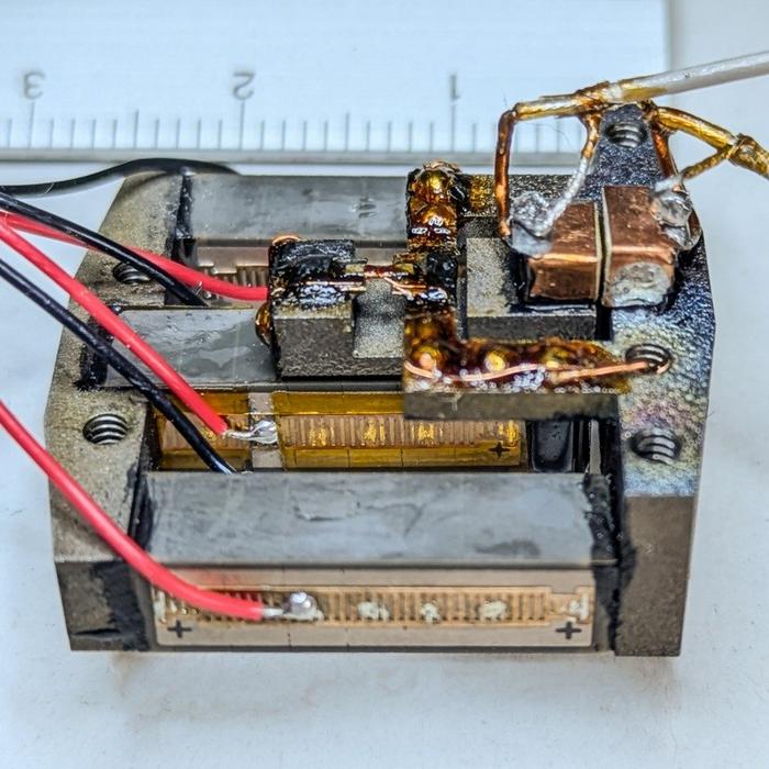
Straining the kagome metal CsV3Sb5 along a single crystallographic axis has revealed two competing superconducting states that are nearly degenerate under ambient conditions. Nuclear quadrupole resonance measurements showed that tensile strain raised the transition temperature from 3.0 K to 3.6 K while leaving charge density wave order essentially intact, decoupling the two phenomena.
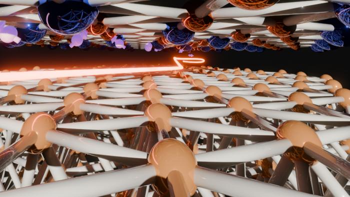
Researchers at the University of Osaka have directly observed a heavy-fermion state forming at the interface between a one-atom-thick ytterbium-copper (YbCu₂) layer and a copper crystal, using intense synchrotron light to probe electron behavior. They identified two distinct states, one confined to the two-dimensional layer and another extending into the three-dimensional substrate, arising from hybridization between localized Yb 4f and mobile conduction electrons.
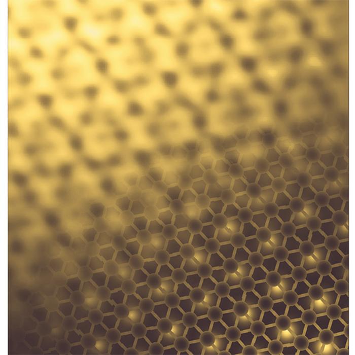
As described in a report in the science journal Nature Materials, the scientists stacked two ultrathin layers of graphene, each a one-atom-thick sheet of carbon atoms arranged in a hexagonal grid. They twisted them slightly atop a layer of hexagonal boron nitride, a hexagonal crystal made of boron and nitrogen. A subtle misalignment between the layers that formed moiré patterns – patterns similar to those seen when two fine mesh screens are overlaid – significantly altered how electrons moved...