Physicists and engineers have found a way to identify and address imperfections in materials for one of the most promising technologies in commercial quantum computing.
The University of Queensland team was able to develop treatments and optimize fabrication protocols in common techniques for building superconducting circuits on silicon chips.
Dr. Peter Jacobson, who co-led the research, said the team had identified that imperfections introduced during fabrication reduced the effectiveness of the circuits.
"Superconducting quantum circuits are attracting interest from industry giants such as Google and IBM, but widespread application is hindered by 'decoherence', a phenomenon which causes information to be lost," he said.
"Decoherence is primarily due to interactions between the superconducting circuit and the silicon chip—a physics problem—and to material imperfections introduced during fabrication—an engineering problem."
"So we needed input from physicists and engineers to find a solution."
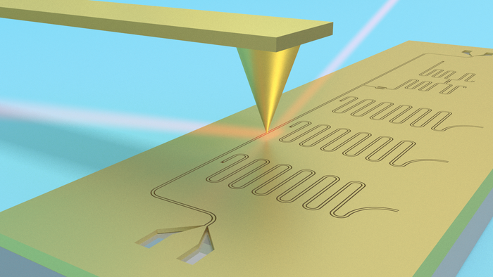
The team used a method called terahertz scanning near-field optical microscopy (THz SNOM)—an atomic force microscope combined with a THz light source and detector.
This provided a combination of high spatial resolution—seeing down to the size of viruses—and local spectroscopic measurements.
Professor Aleksandar Rakić said the technique enabled probing at the nanoscale rather than the macroscale by focusing light onto a metallic tip.
"This provides new access for us to understand where imperfections are located so we can reduce decoherence and help reduce losses in superconducting quantum devices," Professor Rakić said.
"We found that commonly used fabrication recipes unintentionally introduce imperfections into the silicon chips, which contribute to decoherence."
"And we also showed that surface treatments reduce these imperfections, which in turn reduces losses in the superconducting quantum circuits."
Associate Professor Arkady Fedorov said this allowed the team to determine where in the process defects were introduced and optimize fabrication protocols to address them.
"Our method allows the same device to be probed multiple times, in contrast to other methods that often require the devices to be cut up before being probed," Dr. Fedorov said.
"The team's results provide a path towards improving superconducting devices for use in quantum computing applications."
In future, THz SNOM could be used to define new ways to improve the operation of quantum devices and their integration into a viable quantum computer.
Reference
Near-field terahertz nanoscopy of coplanar microwave resonators featured
Xiao Guo, Xin He, Zach Degnan, Bogdan C. Donose, Karl Bertling, Arkady Fedorov, Aleksandar D. Rakić, and Peter Jacobson
