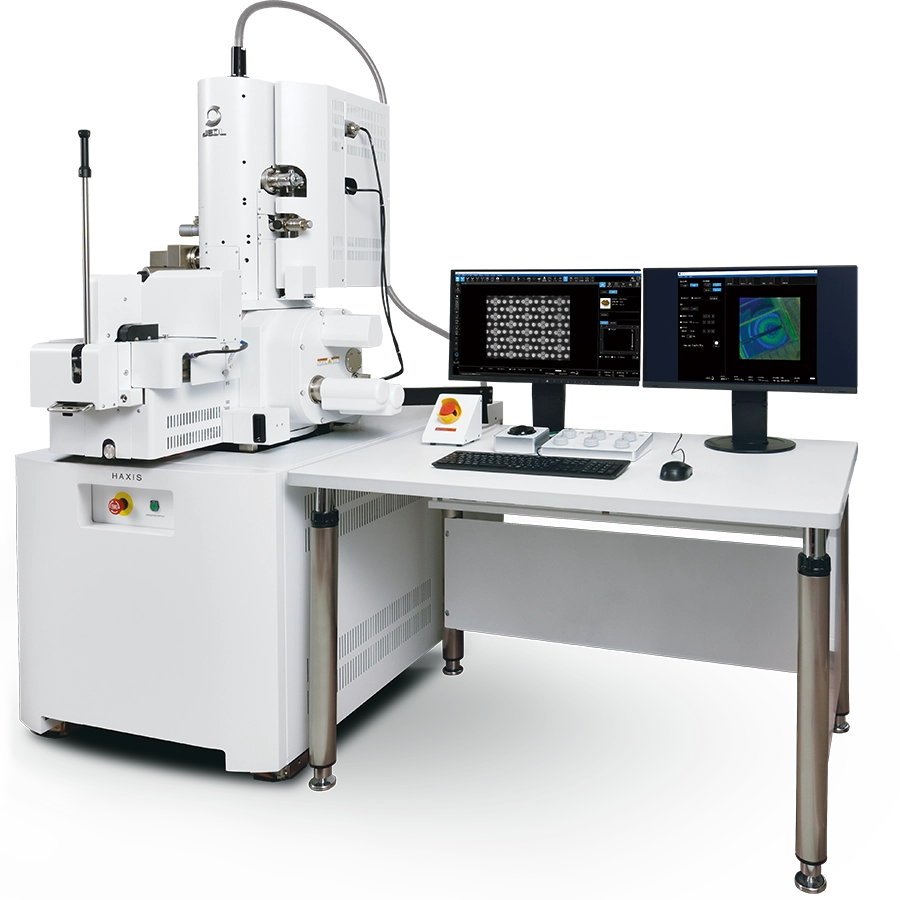
Tokyo, 5 October 2026. JEOL Ltd. has started sales of HAXIS, a scanning electron microscope with low-angle ion milling, designed for semiconductor failure analysis.
As semiconductor structures become smaller and more complex, locating faults by probing circuits with nano-manipulators becomes harder, and probing can affect the sample. HAXIS combines three steps in one system: Low-Angle Ion Milling (LIM), which uses an argon ion beam to remove layers with minimal damage; SEM imaging; and passive voltage contrast (PVC) detection, which locates faults without contact. This allows layer-by-layer analysis of a device.
JEOL lists five main features: clear PVC imaging, cost-effective argon processing, damage-free delayering, layer-by-layer LIM/PVC analysis, and contamination-free sample transfer.
Sales began on 5 October 2026. JEOL's sales target is 15 units per year. The price was not disclosed.
Source: JEOL release via Business Wire
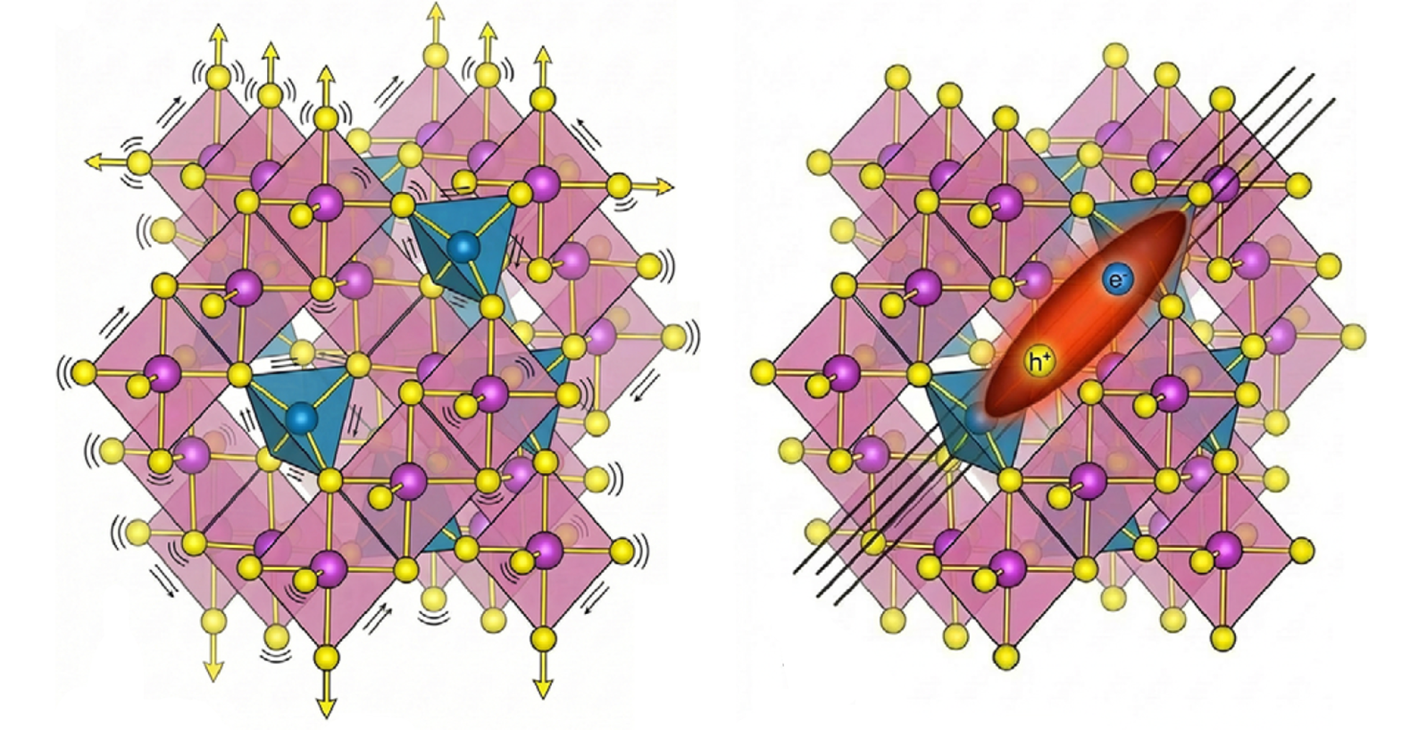
An international research team has demonstrated that the intrinsic disorder of the compound semiconductor CuInSnS₄ can be exploited to influence its optical properties. While the atomic vibrations also sense the local disorder, their response is averaged over many different local environments and therefore appear isotropic, as expected for a cubic crystal. In contrast, the optical excitations, known as excitons, are much more sensitive to the local arrangement of atoms. Surprisingly, they sho...
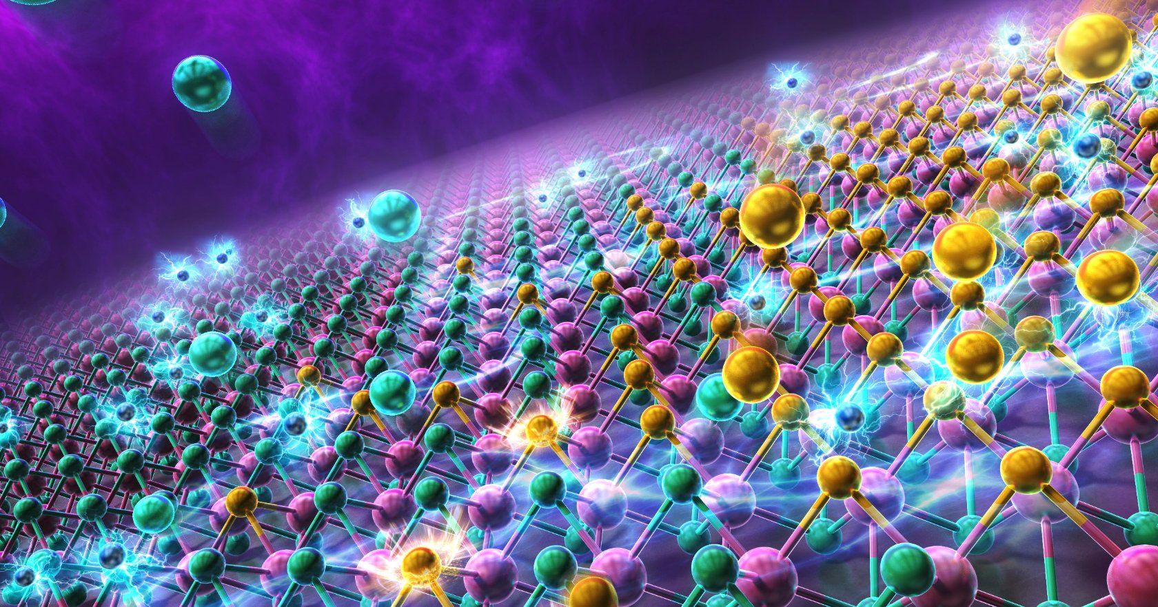
Researchers at Tohoku University have uncovered the long-standing mystery behind the synthesis of Janus two-dimensional (2D) semiconductors, paving the way for more precise manufacturing of materials used in future electronics and clean energy technologies. Janus 2D materials are named after the two-faced Roman god because their top and bottom surfaces are composed of different elements. This asymmetry creates a strong internal electric field, making them attractive for applications such as...
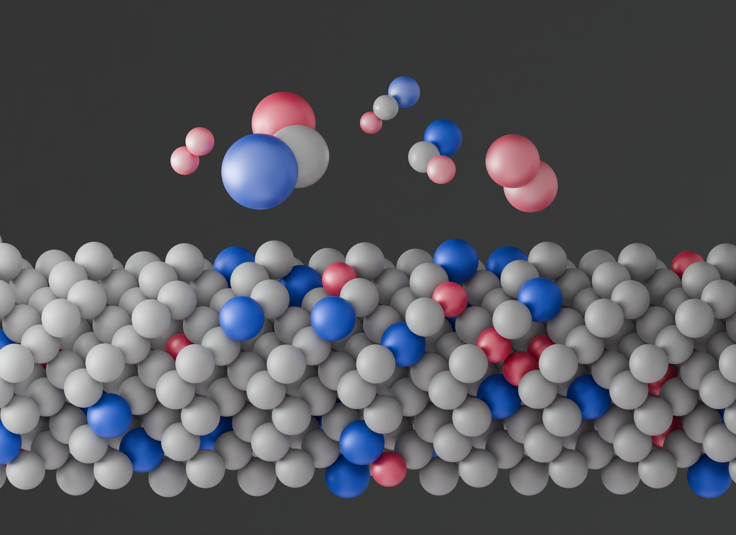
A team led by Lawrence Berkeley National Laboratory (Berkeley Lab) and George Washington University have confirmed that atoms in semiconductors will arrange themselves in distinctive localized patterns that change the material’s electronic behavior. The research, published today in Science, may provide a foundation for designing specialized semiconductors for quantum-computing and optoelectronic devices for defense technologies. On the atomic scale, semiconductors are crystals made of differe...