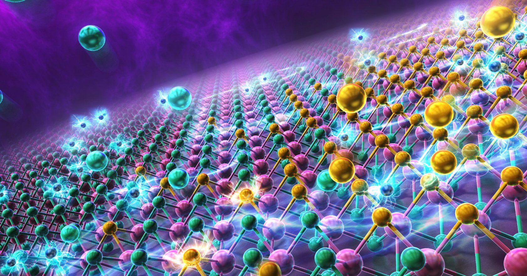
Researchers at Tohoku University have uncovered the long-standing mystery behind the synthesis of Janus two-dimensional (2D) semiconductors, paving the way for more precise manufacturing of materials used in future electronics and clean energy technologies.
Janus 2D materials are named after the two-faced Roman god because their top and bottom surfaces are composed of different elements. This asymmetry creates a strong internal electric field, making them attractive for applications such as photodetectors, solar energy conversion, and hydrogen production.
Despite their potential, Janus 2D sheets have remained difficult to manufacture with precision. Although scientists have been able to create these materials by exposing conventional 2D semiconductors to plasma, the underlying physics was a mystery.
Janus 2D materials are typically synthesized by exposing a conventional 2D semiconductor to plasma, which selectively replaces the top layer of chalcogen atoms with different atoms while leaving the rest of the crystal intact. Still, scientists have long failed to understand the underlying physics behind this process, rendering manufacturing them with precision difficult.
"Atom substitution usually requires immense energy, but this reaction proceeds selectively at room temperature was a puzzle that defied conventional wisdom," said Toshiaki Kato, a professor at Tohoku University's Advanced Institute for Materials Research (WPI-AIMR).
Kato and his colleagues used a newly developed in-situ optical-electrical measurement system to monitor structural and electrical changes during plasma treatment. They discovered that electrons from the plasma accumulate at the interface between the 2D material and its substrate. These excess electrons weaken chemical bonds and lower the energy required for atom substitution, enabling the reaction to proceed efficiently at room temperature.
The team also demonstrated that increasing electron accumulation with ultraviolet light accelerated the reaction by more than twofold. The findings were further validated through first-principles calculations, leading to the development of the "Electron Accumulation Model."
The discovery transforms the synthesis of Janus materials from a trial-and-error process into a predictable, design-based approach. "By controlling the state of accumulated charge, we can now design synthesis processes with unprecedented precision," added Kato.
Because the method does not require high temperatures, it could be applied to flexible plastic substrates, supporting the development of wearable electronics, high-efficiency solar cells, and advanced catalysts for hydrogen and fuel-cell technologies.
Reference
Hidden Role of Electron Accumulation in Driving Room-Temperature Topotactic Substitution for Janus 2D Semiconductors
Dingkun Bi, Tianyishan Sun, Weizi Lu, Hiroto Ogura, Yanlin Gao, Mina Maruyama, Susumu Okada, Toshiaki Kato
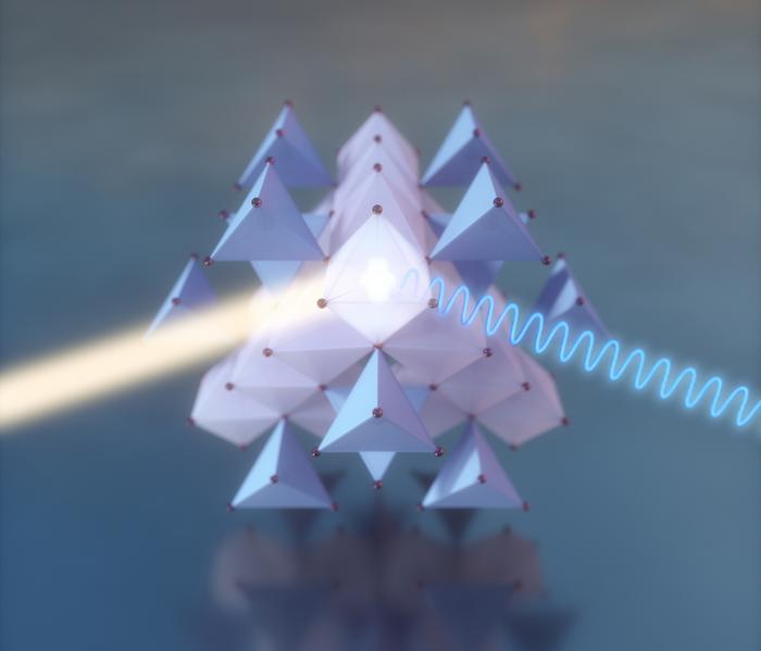
An international research team has observed Jahn-Teller polarons, unique quasiparticles, in cobalt oxide (Co₃O₄) crystals triggered by precisely tailored laser pulses. These polarons emerge through ultrafast electron transfer and local lattice distortions, dramatically influencing the material’s structural, electronic, and magnetic properties. Using advanced pump probe spectroscopy and theoretical modeling led by physicists at the Institute of Nuclear Physics of the Polish Academy of Sciences...
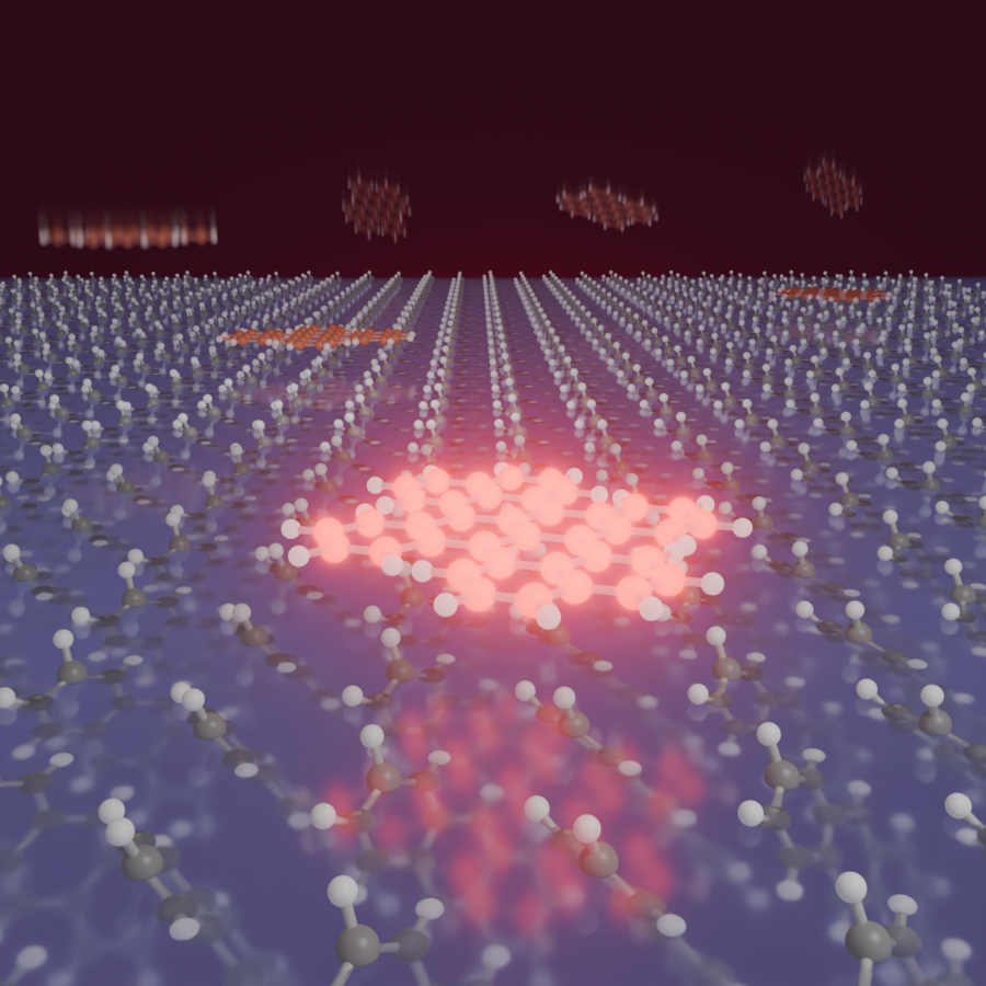
Scientists at the Max Planck Institute for the Science of Light (MPL) have developed a technique for interrogating molecules on surfaces with spectroscopic precision and thereby reaching the ultimate quantum limit for the first time. With their findings, published in Science, the researchers open new opportunities for the study of molecule-surface interactions and molecular quantum technologies.
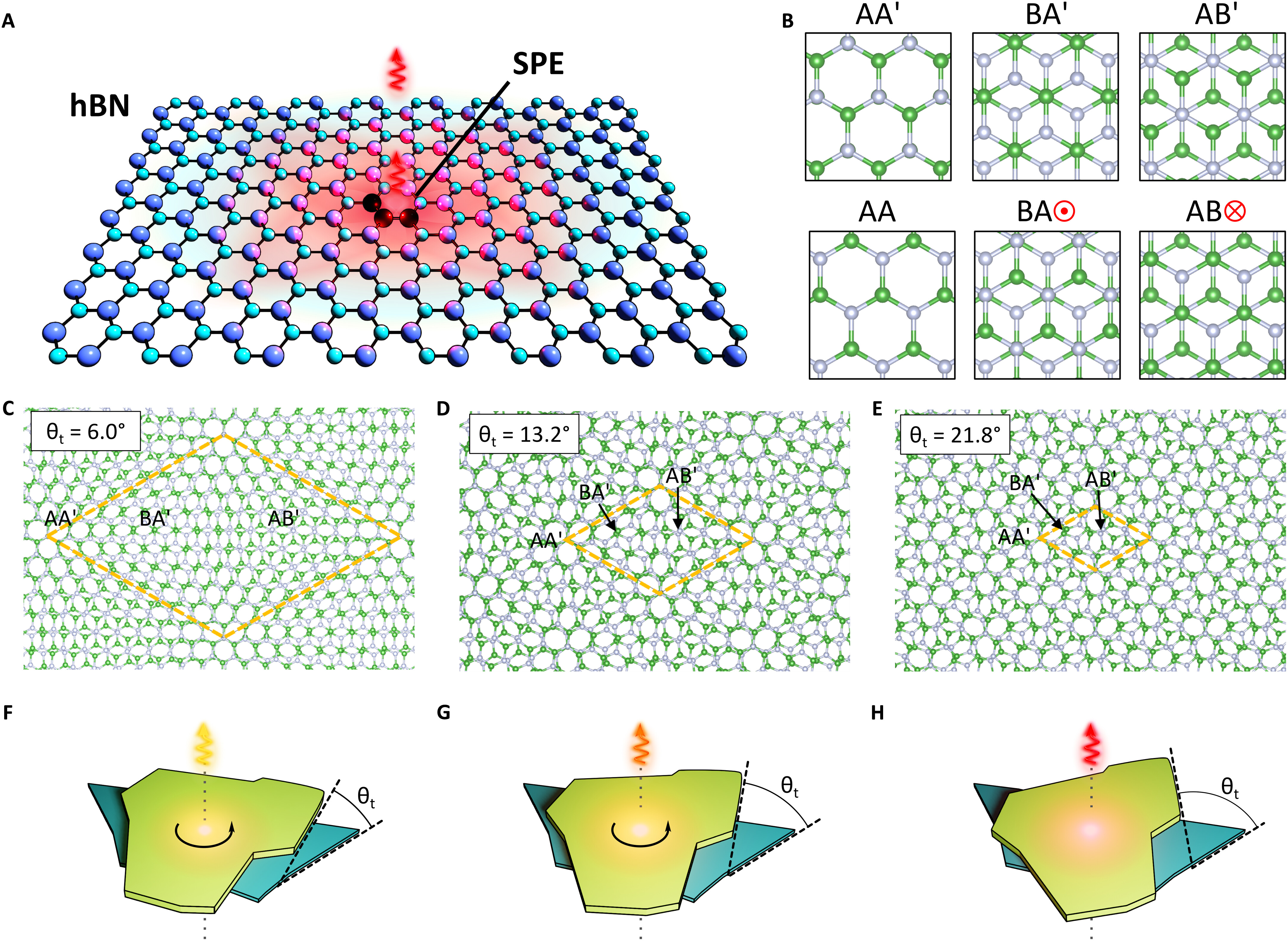
Researchers at the University of Technology Sydney (UTS), in collaboration with the University of Minnesota and Kyung Hee University, have discovered a powerful new way to control tiny quantum light sources by twisting atomically thin layers of hexagonal boron nitride (hBN). In a study published in Science Advances, the team demonstrated that by stacking and twisting hBN layers, they could significantly shift the color and wavelength of quantum emitters. This twistable platform offers far gre...
