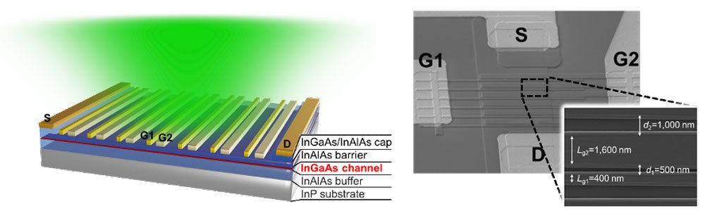
A research group has developed a high-speed, high-sensitivity terahertz-wave detector operating at room temperature, paving the way for advancements in the development of next generation 6G/7G technology.
Details of their breakthrough were published in the journal Nanophotonics on November 9, 2023.
The enhancement of current communications speeds will rely on terahertz (THz) waves. THz waves are electromagnetic waves within the THz range, which falls between the microwave and infrared portions of the electromagnetic spectrum, typically spanning frequencies from 300 gigahertz to 3 THz.
Still, the fast and sensitive detection of THz waves at room temperature is challenging for conventional electronic- or photonic-based semiconductor devices.
This is where two-dimensional plasmons come in. In a semiconductor field-effect transistor, there is a two-dimensional electron channel where a collective charge-density quanta, i.e., two-dimensional plasmons, exist. These plasmons are excited states of electrons exhibiting fluid-like behaviors. Their nonlinear rectification effects, originating from these fluid-like behaviors, and their rapid response (not constrained by electron transit time) make them a promising means to detect THz waves at room temperature.
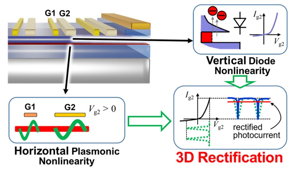
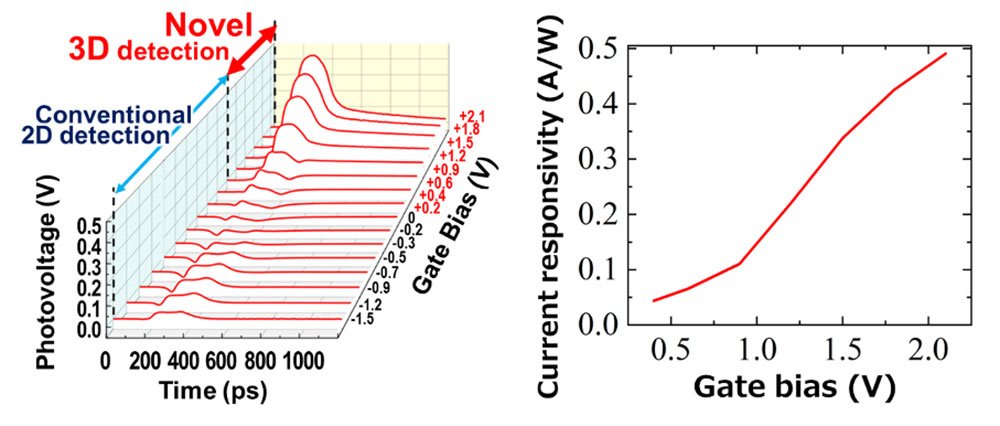
"We discovered a 3D plasmonic rectification effect in THz wave detector," says Akira Satou, leader of the research group and associate professor at Tohoku University's Research Institute for Electrical Communication (RIEC). "The detector was based on an indium-phosphide high-electron mobility transistor and it enabled us to enhance the detection sensitivity more than one order of magnitude higher than conventional detectors based on 2D plasmons."
The new detection method combined the traditional vertical hydrodynamic nonlinear rectification effect of 2D plasmons with the addition of a vertical diode-current nonlinearity.
It also dramatically resolved the waveform distortion caused by multiple reflections of high-speed modulated signals - a critical issue in conventional detectors based on 2D plasmons.
Leading the group alongside Satou was Specially Appointed Professor Tetsuya Suemitsu from Tohoku University's New Industry Creation Hatchery Center and Hiroaki Minamide from RIKEN Center for Advanced Photonics.
"Our new detection mechanism overcomes most of the bottlenecks in conventional terahertz-wave detectors," adds Satou. "Looking ahead, we hope to build on our achievement by improving the device performance."
Reference
Gate-readout and a 3D rectification effect for giant responsivity enhancement of asymmetric dual-grating-gate plasmonic terahertz detectors
Akira Satou, Takumi Negoro, Kenichi Narita, Tomotaka Hosotani, Koichi Tamura, Chao Tang, Tsung-Tse Lin, Paul-Etienne Retaux, Yuma Takida, Hiroaki Minamide, Tetsuya Suemitsu and Taiichi Otsuji
https://www.degruyter.com/document/doi/10.1515/nanoph-2023-0256/html
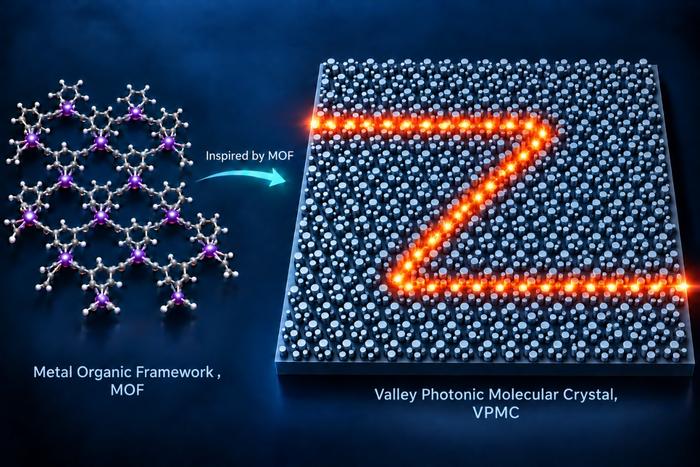
Inspired by Metal-Organic Framework based topological insulators, researchers at Tsinghua University proposed valley photonic molecular crystal (VPMC) and investigated the impact of molecular rotation on the valley-topological properties of VPMC. Credit: Tsinghua University/Xue Feng A research team led by Yidong Huang at Tsinghua University, including Xue Feng and Yongzhuo Li, has developed valley photonic molecular crystals (VPMCs) on a silicon platform. Combining theoretical modeling,...
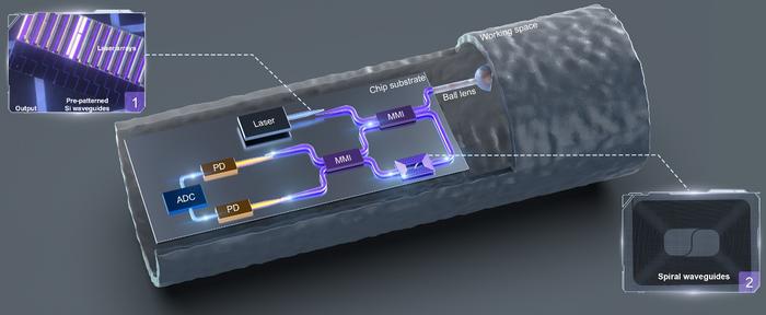
The system integrates a III-V semiconductor light source, SiN-based interferometers, Si-Ge photodetectors (PDs), and an integrated ball-lens microprobe, thereby combining the distinct advantages of multiple photonic integration platforms. The insets illustrate complementary technologies that can be incorporated to realize a miniaturized, fully integrated OCT system. Abbreviations: ADC, analog-to-digital converter. Inset 1: Foundry-scalable embedded III-V lasers on silicon-on-insulator (SOI)...
From left to right: Three photons with different quantum states enter an interferometer with three beam splitters. At each beam splitter, they can take different paths at the same time in superposition. The researchers then measured how often the three photons ended up together at the same output. Counterintuitively, it is possible to make the photons more similar to each other and at the same make them less likely to “bunch” together. AI-generated illustration, by Leonardo Novo. We usually...
