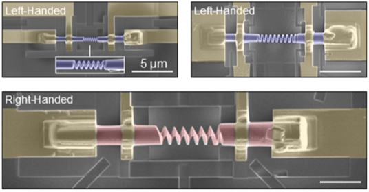
Scientists from the RIKEN Center for Emergent Matter Science and colleagues have developed a new way to fabricate three-dimensional nanoscale devices from single-crystal materials using a focused ion beam instrument. The group used this new method to carve helical-shaped devices from a topological magnet composed of cobalt, tin, and sulfur, with a chemical formula of Co₃Sn₂S₂, and found that they behave like switchable diodes, meaning that they allow electricity to flow more easily in one direction than the other.
Creating complex, three-dimensional nanostructures could help us build more energy-efficient and compact electronic devices. Until now there have been few ways to create such structures, and the currently available methods severely limit the material selection and quality.
In the current study, published in Nature Nanotechnology, the scientists used a focused ion beam that can cut materials with sub-micron precision to overcome this limitation, allowing them, in principle, to shape three-dimensional devices from almost any crystal. In the same way that sculptors use tools to chip away at a material block, they used the ion beam to trim the crystal into a desired shape.
To demonstrate the new method’s power, the researchers used it to create helical devices from a magnetic material, Co₃Sn₂S₂, which they believed, due to its properties, would show a unique diode effect—nonreciprocal electrical transport—arising from the chiral nanoscale geometry. Indeed, they found that the helical devices acted as tiny, switchable diodes: electric current flows more easily in one direction than the other, and this diode effect could be reversed by changing the magnetization or the chiral handedness of the helix. The researchers also found the inverse behavior—strong current pulses can flip the magnetization of the helix. Diodes are important electronic devices used in applications such as AC/DC conversion, signal processing, and LED devices.
By comparing helices of different sizes and temperatures, they traced this effect to the way electrons scatter asymmetrically from the curved, chiral walls of the devices. Together, these results highlight the idea that device shape can be used as a design tool for electronic function, opening new routes to low power, geometry engineered components for future memory, logic, and sensing technologies.
According to Max Birch, the first author of the paper, “By treating geometry as a source of symmetry breaking on equal footing with intrinsic material properties, we can engineer electrical nonreciprocity at the device level. Our newly developed focused ion beam nanosculpting method opens up a wide range of studies on how three dimensional and curved device geometries can be used to realize new electronic functions.”
According to Yoshinori Tokura, the leader of the research group, “More broadly, this approach enables device designs that combine topological or strongly correlated electronic states with engineered curvature in the ballistic or hydrodynamic transport regime. The convergence of materials physics and nanofabrication points to functional device architectures with potential impact on memory, logic, and sensing technologies.”
Source: Riken
Reference
Nanosculpted 3D helices of a magnetic Weyl semimetal with switchable non-reciprocal electron transport
Max T. Birch, Yukako Fujishiro, Ilya Belopolski, Masataka Mogi, Yi-Ling Chiew, Zhuolin Li, Xiuzhen Yu, Naoto Nagaosa, Minoru Kawamura & Yoshinori Tokura
Nature Nanotechnology (2026)
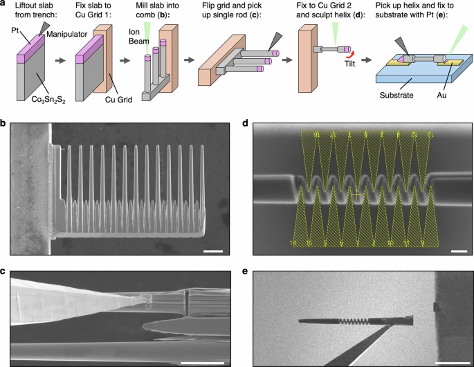
Extended Data Fig. 2 Co 3 Sn 2 S 2 helix device fabrication. @ Nature Scientists from the RIKEN Center for Emergent Matter Science and colleagues have developed a new way to fabricate three-dimensional nanoscale devices from single-crystal materials using a focused ion beam instrument. The group used this new method to carve helical-shaped devices from a topological magnet composed of cobalt, tin, and sulfur, with a chemical formula of Co₃Sn₂S₂, and found that they behave like switchable...
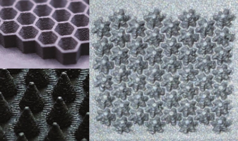
Scientists have created 3D printed surfaces featuring intricate textures that can be used to bounce unwanted gas particles away from quantum sensors, allowing useful particles like atoms to be delivered more efficiently, which could help improve measurement accuracy. The researchers from the University of Nottingham’s School of Physics and Astronomy created intricate, fine-scale surface textures that preferentially bounce incident particles in particular directions. This can help to keep unwa...
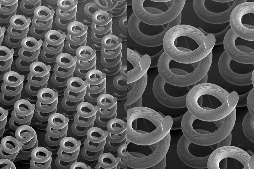
Researchers at Lawrence Livermore National Laboratory (LLNL) have optimized and 3D-printed helix structures as optical materials for Terahertz (THz) frequencies, a potential way to address a technology gap for next-generation telecommunications, non-destructive evaluation, chemical/biological sensing and more. The printed microscale helixes reliably create circularly polarized beams in the THz range and, when arranged in patterned arrays, can function as a new type of Quick Response (QR) for...
