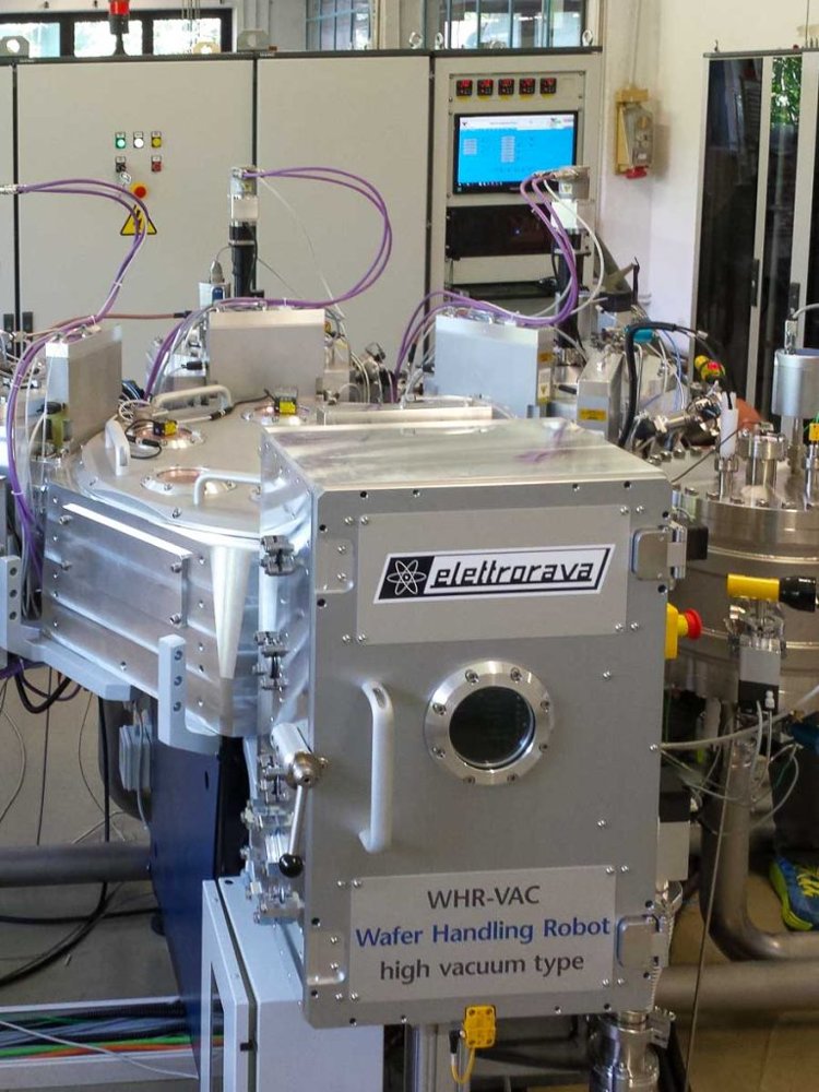
Metalorganic Chemical Vapor Deposition is a method of depositing thin films on a substrate surface through a chemical reaction between one or more reactive gases and the substrate. Using this method is it possible to create high purity dielectric, metallic or semiconducting thin films. In the MOCVD process, ultrapure metalorganic precursor gases are introduced into a reactor, where they undergo pyrolysis on the semiconductor wafer. As a result, the subspecies are absorbed onto the wafer surface. The metalorganic precursor is introduced into the process chamber via a system known as "bubbler", which uses an inert carrier gas (such as He or Ar) to transport the precursor liquid into the chamber. MOCVD operates at moderate pressures (1 to 760 Torr) in the gas phase. Applications: MOCVD is commonly used in the production of laser diodes, LEDs, and semiconductors for advanced optoelectronics, high power and highspeed electronics, enabling mass production of semiconductor heterostructures via bandgap engineering. Furthermore, MOCVD can be utilized to precisely fabricate 0D, 1D, and 2D nanomaterials. - Consumer Electronics - Solar energy - Aerospace and Defence - Healthcare and medical devices - Optics and Photonics - Power Electronics - Research Key features: - Metalorganic liquid precursors - HV or UHV configuration - Reactive gases (SiH4, NH3, H2, CH4, N2, etc.) and/ or liquid precursors controlled directly from the software - Optional vapor source controller for liquid Precursor with tank/cylinder in a closed cabinet for safe refill - Optional single or multiple automatic or manual load lock with optional pre-heating and/or plasma treatments - Optional wide range optical thickness monitor for the control of layer thickness Deposited materials: Oxides, Nitrides, Carbides, Semiconductors, Carbon Based Materials, Organics Metalorganic CVD - the best choice for obtaining compound materials with finely tailored composition starting from liquid precursors
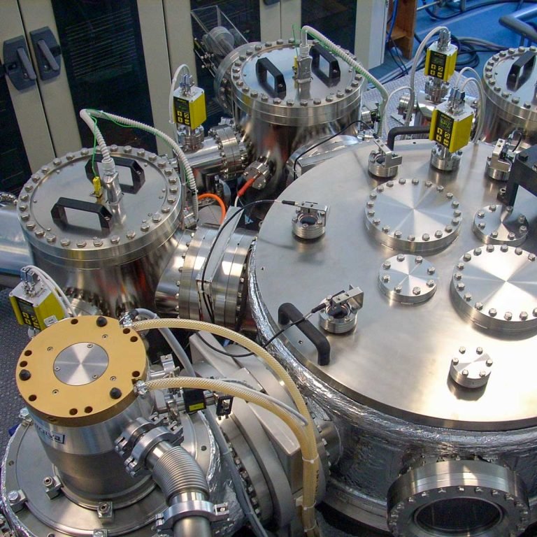
Plasma-enhanced chemical vapor deposition is a plasma-based deposition method used to deposit material on a substrate surface. PECVD is commonly used for depositing silicon oxide/nitride, hydrogenated amorphous and microcrystalline silicon and carbon, Diamond-like carbon (DLC), semiconductors and oxides. The process involves introducing a gas mixture into the vacuum chamber, where a plasma is generated. The process gases are ionized and decomposed into ions and radicals, which react with the substrate via chemical reactions, leading to the deposition of a thin film on the substrate. The plasma can be generated using different methods such as radio frequency (RF), alternating current (AC), or direct current (DC) discharge between two electrodes. PECVD offers a higher deposition rate while maintaining a lower temperature compared to thermal CVD Applications PECVD is used to produce high-quality semiconductor and dielectric films required for various applications, like low and high-power semiconductor devices, photovoltaic solar cells' active layers, metal-insulator-metal (MIM) capacitors, laser diodes, sensors, detectors, LEDs, thin film transistors, and more. - Consumer Electronics - Automotive Industry - Solar energy - Aerospace and Defence - Healthcare and medical devices - Optics and Photonics - Wear resistant coatings Key features - RF showerhead electrode for uniform electric field and gas distribution - Modular process gas manifold with mass flow controllers for up to 12 gases - Optional vapor source controller for liquid Precursor (i.e. TEOS) with tank/cylinder in a closed cabinet for safe refill - Automatic process pressure control - Alternatively Hot Wire CVD - In situ spectroscopic plasma monitoring - Optional automatic or manual load lock (optional pre-heating and/ or plasma treatments) - Optional wide range optical thickness monitor for the control of layer thickness - Optional in situ spectroscopic ellipsometry for thickness measurement Deposited materials Metals, Oxides, Nitrides, Carbides, Semiconductors, Carbon Based Materials, Organics Plasma Enhanced CVD - the right choice for obtaining large area compound materials mixing gaseous and/or liquid precursors at any temperature
CATEGORY
Plasma-enhanced chemical vapor deposition is a plasma-based deposition method used to deposit material on a substrate surface. PECVD is commonly used for depositing silicon oxide/nitride, hydrogenated amorphous and microcrystalline silicon and carbon, Diamond-like carbon (DLC), semiconductors and oxides. The process involves introducing a gas mixture into the vacuum chamber, where a plasma is generated. The process gases are ionized and decomposed into ions and radicals, which react with the substrate via chemical reactions, leading to the deposition of a thin film on the substrate. The plasma can be generated using different methods such as radio frequency (RF), alternating current (AC), or direct current (DC) discharge between two electrodes. PECVD offers a higher deposition rate while maintaining a lower temperature compared to thermal CVD Applications PECVD is used to produce high-quality semiconductor and dielectric films required for various applications, like low and high-power semiconductor devices, photovoltaic solar cells' active layers, metal-insulator-metal (MIM) capacitors, laser diodes, sensors, detectors, LEDs, thin film transistors, and more. - Consumer Electronics - Automotive Industry - Solar energy - Aerospace and Defence - Healthcare and medical devices - Optics and Photonics - Wear resistant coatings Key features - RF showerhead electrode for uniform electric field and gas distribution - Modular process gas manifold with mass flow controllers for up to 12 gases - Optional vapor source controller for liquid Precursor (i.e. TEOS) with tank/cylinder in a closed cabinet for safe refill - Automatic process pressure control - Alternatively Hot Wire CVD - In situ spectroscopic plasma monitoring - Optional automatic or manual load lock (optional pre-heating and/ or plasma treatments) - Optional wide range optical thickness monitor for the control of layer thickness - Optional in situ spectroscopic ellipsometry for thickness measurement Deposited materials Metals, Oxides, Nitrides, Carbides, Semiconductors, Carbon Based Materials, Organics Plasma Enhanced CVD the right choice for obtaining large area compound materials mixing gaseous and/or liquid precursors at any temperature
CATEGORY
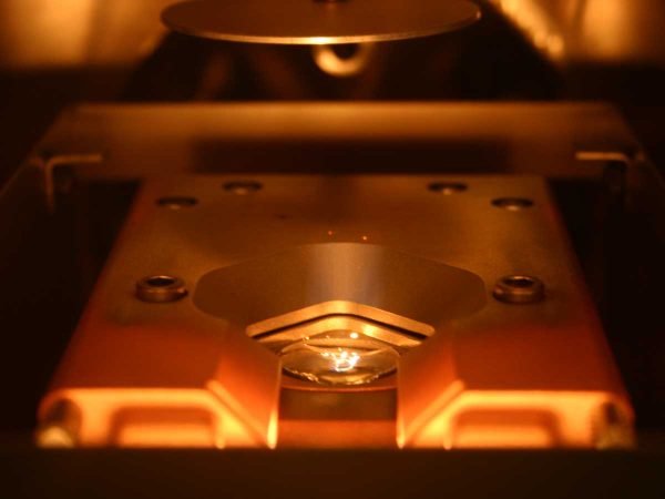
Electron Beam Evaporation (EBPVD) is a physical deposition technique used to create thin films on a substrate surface by evaporating a solid material placed in a crucible. The e-beam is generated through the thermionic emission process, where an electric current passes through a tungsten filament, causing the filament to heat up and emit electrons. High voltage is then applied between the filament and the hearth, allowing the liberated electrons to accelerate towards the crucible, while a magnetic field focuses them into a beam. The collimated electron beam hits the material in the crucible, allowing the evaporation process and the aggregation on the substrate surface. Compared to thermal PVD, EBPVD allows high evaporation temperature materials deposition as thin films. Deposition rates using electron beam processes can vary from 1 nm per minute to several μm per minute, depending on the required structural and morphological film control. Applications E-beam evaporation finds widespread use in various industries, like semiconductor, thin-film solar, aerospace, and cutting and tool industries, for producing wear-resistant and thermal barrier coatings. This technique is used also to produce dielectric, optical coatings, and Josephson junctions and in micro and nano-fabrication for lift-off processes. - Automotive Industry - Consumer Electronics - Aerospace and Defence - Healthcare and medical devices - Optics and Photonics - Energy storage Key features - OHFC copper hearth crucible with up to 8 pockets of various sizes - HV or UHV configuration - Fully integrated quartz crystal controller for the automatic control of the thickness - Optional reactive gases, such as oxygen or nitrogen useful to reactively deposit non-metallic films - Optional automatic or manual load lock with optional pre-heating and/or plasma treatments - Optional ion beam source for bombarding the substrates during deposition (Ion Beam Assisted Deposition - IBAD) - Evaporation sources come in various sizes and configurations, single or multiple pockets Deposited materials Metals, Oxides, Nitrides, Carbides, Semiconductors
CATEGORY
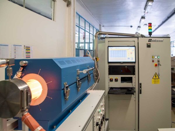
Thermal Low Pressure Chemical Vapor Deposition (TLPCVD) is a method of depositing thin films on a substrate surface through a thermally activated chemical reaction between one or more reactive gases and the substrate. This deposition technique is used for the deposition of silicon, silicon dioxide, silicon nitride and for the production of carbon nanotubes and graphene. In thermal CVD process, the precursor gas molecules are introduced into a heated chamber in vacuum atmosphere, reacting with the substrate surface at high temperatures, depositing a thin film of the desired material onto the substrate. The substrate is heated to provide the energy needed for precursor reaction and/or decomposition, because the high temperature enables the gas to react with the substrate, improving crystallinity and density of the thin film Applications Thermal CVD is a common method for depositing various materials including Silicon Oxide (SiO 2 ), Silicon Nitride (Si 3 N 4 ), Silicon Carbide (SiC), transition metal oxides (Ta 2 O 5, TiO 2, and ZrO 2 ), transition metal silicates (SiO 2 )–(ZrO 2 ) alloys, and carbon-based materials like graphene and carbon nanotubes. - Consumer Electronics - Aerospace and defence - Healthcare and medical devices - Optics and photonics - Energy storage - Catalysis Key features - Hot Wall CVD or LPCVD configuration, up to 1200 °C. Precise and auto tuneable temperature control with completely settable ramp parameters - Single or multiple furnaces in Hot Wall or Quartz Tube configuration - Reactive gases (SiH 4, NH 3, H 2, CH 4, N 2, etc.) and/ or liquid precursors controlled directly from the software - Optional vapor source controller for liquid Precursor with tank/cylinder in a closed cabinet for safe refill - Optional single or multiple automatic or manual load lock with optional pre-heating and/or plasma treatments Deposited materials Oxides, Nitrides, Carbides, Semiconductors, Carbon Based Materials, Organics Thermal Low Pressure CVD a reliable and affordable technology for a wide range of deposited materials
CATEGORY
