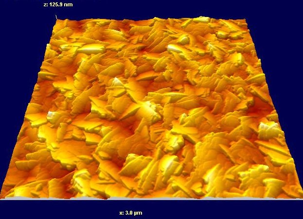
AFM scan of a TipCheck calibration surface showing the sharp, randomly-oriented peaks which provide the optimal surface for characterizing AFM tip geometry. Why Tip Check? When imaging a new sample in an AFM, it may be difficult to know whether one has obtained an accurate representation of the surface. Even in the case that a fairly clear idea of expected feature topography exists, an independent means of assessing the influence of the probe tip on the image is desirable. Consider the following: - A broken or misshapen probe tip results in inaccurate rendering of samples. Extra time from an already busy schedule can be consumed in further clarification work that wouldn’t have been needed otherwise. Worse, if the tip damage goes undetected, the true topographical nature of your samples may inadvertently go unnoticed. - Using microscopy techniques such as SEM to look for breakage in tips is neither convenient nor economical enough to be done routinely. A simple, convenient means to prescreen all of one’s AFM tips is certainly desirable! You and your team can thereby save time and effort, and avoid frustration. Fortunately, there is a simple and effective means to prescreen your tips, and assess used tips as well. TipCheck exploits reverse imaging to provide a fast and simple way to assess new and used tips without the need for SEM inspection. TipCheck helps you to categorize and permit qualitative comparisons between tips. The microstructure of the TipCheck film is ideal for the detection of tip morphology in the vicinity of the tip apex. The AFM images shown here were obtained by imaging a TipCheck surface with a broken tip (left) and a reasonably good tip (right). The film is supplied on a chip of silicon, ready to be placed in your AFM. Instructions are provided with examples of images to aid you in getting started with your own sample library.
