By Lam Research
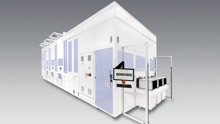
Strip and clean techniques are used between manufacturing steps to eliminate unwanted material that could later lead to defects and to prepare the wafer surface for subsequent processing. Photoresist strip removes the photoresist film and residues following ion implant or etch steps. To clear away particles, contaminants, residues, and other unwanted materials, wafer cleaning steps are inserted throughout manufacturing. Wet processing technologies can be used for wafer cleaning as well as strip and etch applications. Plasma bevel cleaning is used to enhance die yield by removing unwanted materials from the wafer’s edge that could impact the device area. Our strip technologies selectively remove remaining photoresist and provide process flexibility for multiple applications, while our high-productivity clean products deliver pristine surfaces center to edge for the most demanding cleaning steps.
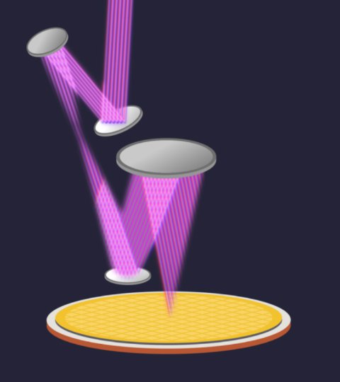
In the race to power artificial intelligence and edge computing, the semiconductor industry faces an unprecedented challenge: creating chips with impossibly small features while ensuring every microscopic component lands precisely where it should. The industry’s ability to deliver these innovations depends on our ability to manufacture chips at ever-smaller nodes in higher volumes. This challenge manifests acutely in the patterning process — the crucial stage where microscopic circuit designs are transferred onto silicon wafers. A Revolutionary Approach to Advanced Patterning Aether, our groundbreaking dry resist technology, fundamentally reimagines the resist process with dry processing, which breaks several key tradeoffs in the printing of microscopic circuit designs on wafer. With this pristine, vacuum-based approach, Aether extends single print patterning. This reduces both the cost and complexity of creating the intricate patterns required for next-generation chips. Additionally, the technology’s metal-organic compounds absorb three to five times more light during extreme ultraviolet (EUV) lithography than traditional carbon-based resist materials, dramatically lowering the cost while improving performance. Features + Benefits - Enhanced photon absorption and precision patterning capabilities enable manufacturers to maintain single print patterning at advanced nodes. - Contrast to traditional methods of double patterning, which costs 1.5-2x more than single print patterning. - Reduced process steps and extending single print pattern fidelity, Aether streamlines production flows, which translates to higher yields. - Improved precision enables the creation of denser, faster memory arrays that can keep pace with AI’s growing appetite for data. - Dramatically reduced chemical usage, creating a more environmentally friendly solution. Lam’s dry resist technology represents a fundamental rethinking of how we create the building blocks of modern computing. Aether, when combined with Lam’s suite of advanced patterning solutions for EUV patterning, enables patterning at the lowest cost to the industry, ultimately pushing the boundaries of physics and delivering on the future of AI.
CATEGORY
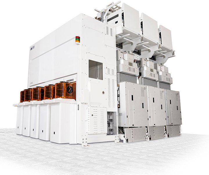
Future device architectures will require etching capabilities that exceed even the most advanced plasma etch technologies available today to enable the AI era. New logic transistors, such as CFETs, and new memory architectures, such as 4F2 and 3D DRAM, demand new extremes in etching performance to shape and form increasingly precise 3-dimensional structures that must be perfectly matched trillions of times across a single 300mm wafer. To solve the challenges in forming these 3D devices, IC manufacturers will need a generational boost to their plasma etching capability. Building on over two decades of conductor etch market leadership, Akara® is a revolutionary leap forward. Akara® features the first use of a solid-state plasma source, called DirectDrive®, to deliver etch process control and responsiveness not previously feasible. DirectDrive® responds to the process changes needed to form complex 3D structures over 100x faster than previous plasma sources. When combined with proprietary ion energy control and plasma pulsing systems, Akara® delivers the performance needed for future CFET logic transistors and 3D DRAM channels. Designed for high-volume production with maximum process yield, Akara® increases wafer output and eliminates wasted time, with millisecond response times to any change. The industry’s most advanced etch uniformity controls provide angstrom-level critical dimension uniformity and wafer to wafer repeatability. Building on the legacy and experience from over 30,000 Kiyo chambers in production, Akara: 1. Enables ultra-small space etches with higher aspect ratio and critical dimensions — doing it with ultra-precision at industry-leading speed. 2. Is designed for improved sustainability, efficiency and total cost of ownership. - New plasma source technology and better etching efficiency reduces the energy footprint associated with making chips. Building on the legacy of Kiyo®, Akara® represents the next chapter in Lam’s history of conductor etch innovation and leadership, delivering advanced technology to meet future demands. Product Offerings: Sense.i® Platform Key Applications: 3D NAND, CFET, 3D DRAM
CATEGORY
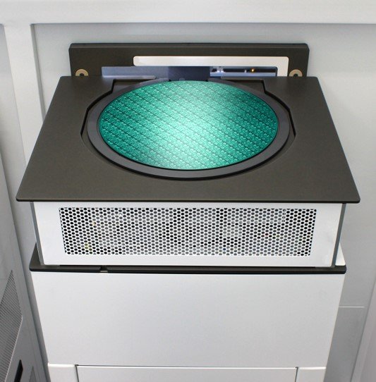
In-line process monitoring is used to identify production wafer trends and excursions as they occur, allowing corrections to be implemented quickly to prevent further yield loss. For deposition, etch, and clean steps, measurement of the mass change of a wafer before and after a process is a simple and direct means of monitoring and controlling process results, particularly for ultra-thin films, ultra-thick films, and complex 3D geometries of newer chip designs, where traditional optical metrology techniques are ineffective. Lam’s Metior® mass metrology systems, available as both platform-integrated modules and as stand-alone systems, deliver sub-milligram mass measurement capability for advanced process monitoring and control of three-dimensional device structures. Industry Challenges As devices become more three-dimensionally complex, traditional optical metrology techniques are often insufficient for maintaining tight control of etch, deposition, and clean processes. For example, the bottoms of high aspect ratio (HAR) structures may be invisible to top-down optical signals. Likewise, certain thick films are frequently too opaque for precise thickness measurement, and lateral processing steps occur too deeply in a structure to be visible. Many geometries are now so complex that fitting optical critical dimension (OCD) models requires substantial investment and long development and validation timelines. In addition, meeting tight requirements for etch applications often requires real-time methods for addressing within-lot and lot-to-lot variability sources. As a result, chipmakers require an alternative means of monitoring process results that addresses the limitations of optical techniques in a cost-effective manner. Key Customer Benefits - Low cost of ownership, high-throughput in-line process monitoring - Simple measurement with clear physical meaning (wafer mass and mass change) - High sensitivity with sub-nanometer film detection capability - Greater sensitivity as device complexity and aspect ratio increases - Process control on 3D/hidden structures where optical metrology is ineffective - Maximum flexibility for multi-application use and variable sampling strategies using standalone system configuration - Real-time control and lower cost of sampling on every wafer using platform-integrated configuration Product Offerings - Metior® HX - Metior® HXE Key Applications - HAR etch – DRAM cell, 3D NAND channel hole - Conformal and ALD/sidewall deposition - Horizontal processing –recess etch, fill - Film density monitoring - Carbon mask open - Wafer cleaning/polymer removal
CATEGORY
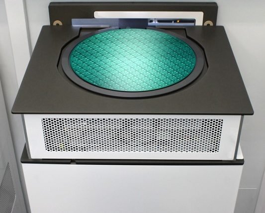
Mass Metrology measures the change in mass following deposition, etch, and clean processes to enable monitoring and control of these often-repeated core manufacturing steps. This measurement enables Å-level quantification to process changes. Especially for processes involving high aspect-ratio structures, complex 3D architectures, OR Atomic Layer Deposition, optical techniques are limited in their ability to measure accurately the thick, deep, or otherwise visually obscured features. Measuring the change in mass for these applications provides a simple, accurate, high-precision yet high throughput solution for monitoring and control of the critical features in advanced device processes, where there is often little tolerance for variation. Our line of high-precision mass metrology systems provides in-line monitoring and control of nearly all wafer-processing steps in real-time. Mass measurement is capable of recording minute changes on the wafer (incl. Queue time effect) in maximizing outlier detection while optimizing Metrology fleet investment.
CATEGORY
