By LayTec GmbH
automated wafer mapping – Automated white light reflectance (WLR) and photoluminescence (PL) wafer mapping – Post-process quality control of entire wafer area with EpiX® – Extended spectral range 250–2400 nm – Spectral resolution down to 0.1 nm – XY mapping stage with automated wafer thickness compensation – Up to 4 configurable laser wavelengths – Adjustable laser power – Predefined and customized algorithms – Up to two load ports for 3", 100 mm, 150 mm & 200 mm cassettes – Prealigner (optional) – Wafer-ID Reader (optional) – Fan-Filter-Units (optional) – Industry-compatible clean room design (up to ISO 3) – High throughput – Automated normalization of measurement data – Wide set of standard analysis methods – Automated yield analysis – Combination of complementary in-situ and ex-situ metrology for in-depth and areal wafer analysis through Combining white light reflectance and photoluminescence, the EpiX® C2C system ensures a comprehensive 2D analysis of critical wafer properties by non-contact optical measurements. The cassette-to-cassette configuration of EpiX® C2C allows to achieve the high throughput required in industrial applications. Parameters Mapping Stage XY scan area ≤ 200 mm diameter Normalization (WLR & PL) Automatic using reference sample Sample holder Continuous vacuum chuck Wafer thickness compensation Distance sensor & z-stage (optional) Mapping speed 100 mm wafer @ 1.0 mm pitch 200 s Mapping speed 150 mm wafer @ 2.0 mm pitch 150 s Photoluminescence Measurements Up to 4 laser sources configurable Default: 405 nm, 532 nm, 785 nm, other wavelengths upon request Laser power on sample for default setup 405 nm: > 25 mW | 532 nm, 785 nm: > 80 mW Intensity stability across wafer < ± 3 % Signal to noise within single spectrum < ± 1 % Spectroscopic Reflectance Measurements Optical head Combined optical head for WLR and PL measurements Spot size configurable: 100 μm, 200 μm, 300 μm WLR light source Tungsten lamp 2915 K (alternative UV light source available) Spectral range configurable: 230 nm to 2400 nm Spectral resolution ≥ 0.1 nm, depending on grating Number of gratings Up to 4 Alternative spectrometer configuration Multiple fixed spectrometers measure in parallel Absolute accuracy at wafer center < ± 0.5 % Signal to noise within single spectrum < ± 0.5 % System-induced deviation across wafer < ± 0.5 % Analysis Features – Edge exclusion – Virtual rotation – Predefined and customized – VCSEL analysis – Single film thickness/composition – Multi peak analysis (analytic/numeric) – Wafer thickness – Full spectral fitting (+connected metrology option) – Die pattern assignment – Import of customer die layout – Wafer level – Die level – XML reports, PDF reports, ASCII exports Software modifiers Algorithms Virtual die patterns Automated yield analysis Reports Parameter Basic Options Load ports 1 Up to 2 Cassette type Open cassette Open cassette, SMIF, FOUP Wafer size 3", 100 mm, 150 mm & 200 mm 3", 100 mm, 150 mm & 200 mm (other sizes upon request) Prealigner Software alignment Optional Wafer ID reader Optional, from above and below Fan-Filter-Unit Optional – Stop band: center, width, edges, height – FP-Dip: center, width, height, area – Identical to in-situ analysis in EpiNet for EpiTT VCSEL – Peak types: Gauss, Lorentz, numeric analysis – Output results: peak wavelength, center wavelength, centroid wavelength, dominant wavelength, height, width, area, asymmetry Options White light reflectance and VCSEL analysis Photoluminescence & multi peak analysis Layout Manual Loading Access Height: 2350 mm Length: 1650 mm Width: 1300 mm Width: 1300 mm Length: 1650 mm Load Ports Control PC Prealigner Wafer Handler Wafer ID-Reader XY-Wafer Stage EpiX ® C2C is designed with multiple upgrade options: extended wavelength range, software interfaces (e.g. for user-owned spectral analysis libraries) upon request. Dimensions & Connections Footprint (WxDxH) ~ 1300 x 1650 (+300) x 2500 mm Mass ~ 1400 kg Power supply 230 V / 16 A CEE 7/4 (CE version) 208 V / 20 A (international / UL version) Vacuum 8 mm, if present, else internal vacuum option available Network RJ45 Operating conditions Clean room or comparable laboratory, temperature 22 ± 2 °C, humidity < 55 % Laser classification CLASS 1 LASER PRODUCT according to DIN-EN60825-1:2015-07 Specifications are subject to further technical development and may differ from those given in the data sheet. Please consult our technical sales team to see how LayTec metrology can best serve your specific application. Developed, manufactured and qualified in Germany.
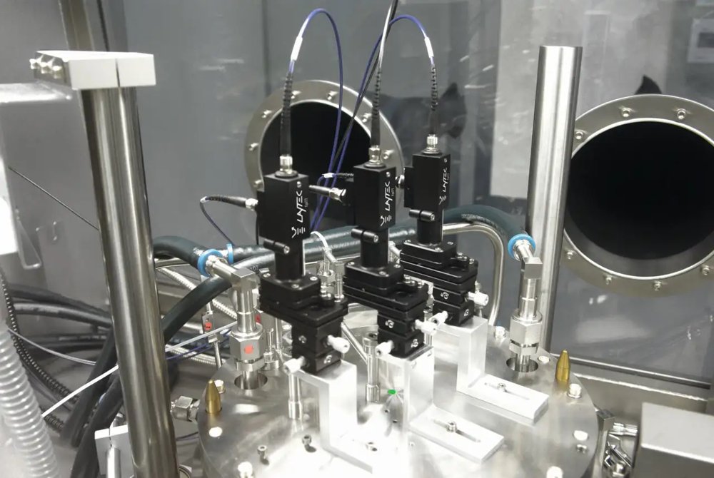
Combine measurements of temperature and reflectance at three wavelengths in one tool. EpiTT combines measurements of temperature and reflectance at three wavelengths in one tool. For True Temperature (TT), we apply the method of emissivity corrected pyrometry, which delivers the precise surface temperatures of opaque materials at 950 nm (Si, GaAs, InP). For materials that are transparent at 950 nm (GaN, Sapphire, SiC), EpiTT measures the temperature on the top side of the carrier. Measuring reflectance at three wavelengths monitors all essential properties of the growing layers, such as growth rate, film thickness, stoichiometry changes and morphology. EpiTT offers industry standard metrology for all kinds of epitaxial growth systems and is compatible with different main rotation frequencies in the range from 5-1500 rpm. Fields of application - Temperature range: T=450°C to 1300°C for large viewport systems/T=500°C to 1400°C for narrow viewport systems/other temperature ranges on request, e.g. 1500°C for UV LED applications, 1700°C for SiC - Wafer temperature with precision better than ±1K in a range of 600°C to 1400°C - Wafer and area selective measurements - True wafer temperature for opaque semiconductors such as InP, GaAs and Si - Pocket temperature for GaN, Sapphire and SiC Product features Emissivity corrected pyrometry: - Temperature range from 450°C to 1300°C for large viewport systems/500°C to 1400°C for narrow viewport systems / other temperature ranges on request, e.g. 1500°C for UV LED applications, 1700°C for SiC - Accuracy better than 1 K - Wafer and area selective measurements - True wafer temperature for opaque semiconductors such as InP, Graphite (SbS) - Pocket temperature for GaN, Sapphire and SiC Reflectance at three wavelengths: - 950 nm, 633 nm and 405 nm - Growth rate, layer thickness, roughness and other layer qualities - Full performance up to 1500 rpm main susceptor rotation - Further wavelength (e.g. 280nm, 365nm, 1550nm) for special applications are available on request
CATEGORY
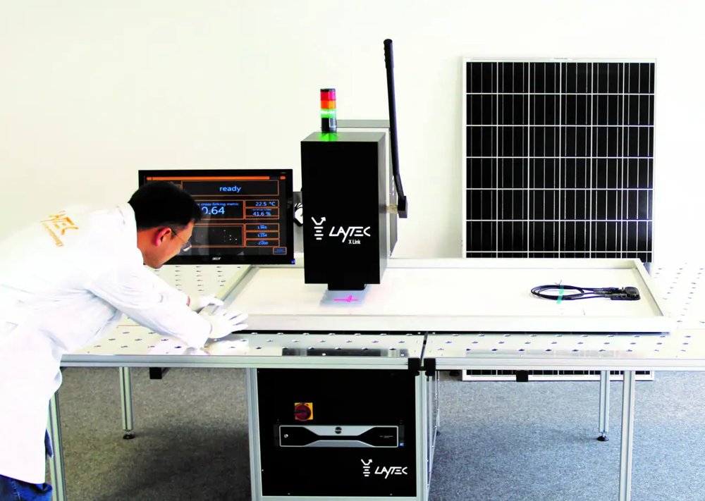
X Link® enables fast, automated, non-destructive and accurate evaluation of the level of EVA or polyolefin cross-linking in PV module encapsulation processes. In solar modules, the ethylene vinyl acetate (EVA) or polyolefin encapsulation protects the sensitive solar cells from the environment. In consequence the degree of intermolecular cross-linking of EVA or polyolefin is decisive for the long-term stability and performance of a module. Cross-linking is achieved by thermally curing the polymers during the lamination process. The X Link® system enables fast, automated, non-destructive and accurate evaluation of the level of EVA or polyolefin cross-linking immediately after lamination. It can be integrated into any solar module production site, offering a flexible platform for encapsulation quality control ranging from single point sampling to full module mapping. The stand-alone version is designed for lab applications, manual product sampling, areal mappings, R&D labs and pilot lines, ready to test full-size production-type modules with or without frames. High-resolution spatial mappings of the cross-linking degree and statistical evaluation can be performed. Furthermore, the manual off-line version allows multiple-point measurements on laminates and out-of-production modules, and modules from the field. This setup is a highly useful quality control tool for incoming goods inspection for EPCs, certifiers and consultants. Fields of application - Module encapsulation quality control in glass/backsheet solar module production Product features - Non-destructive test procedure - Testing time of only seconds per measurement points - Flexible module mapping capability - Data output in “% gel content”
CATEGORY
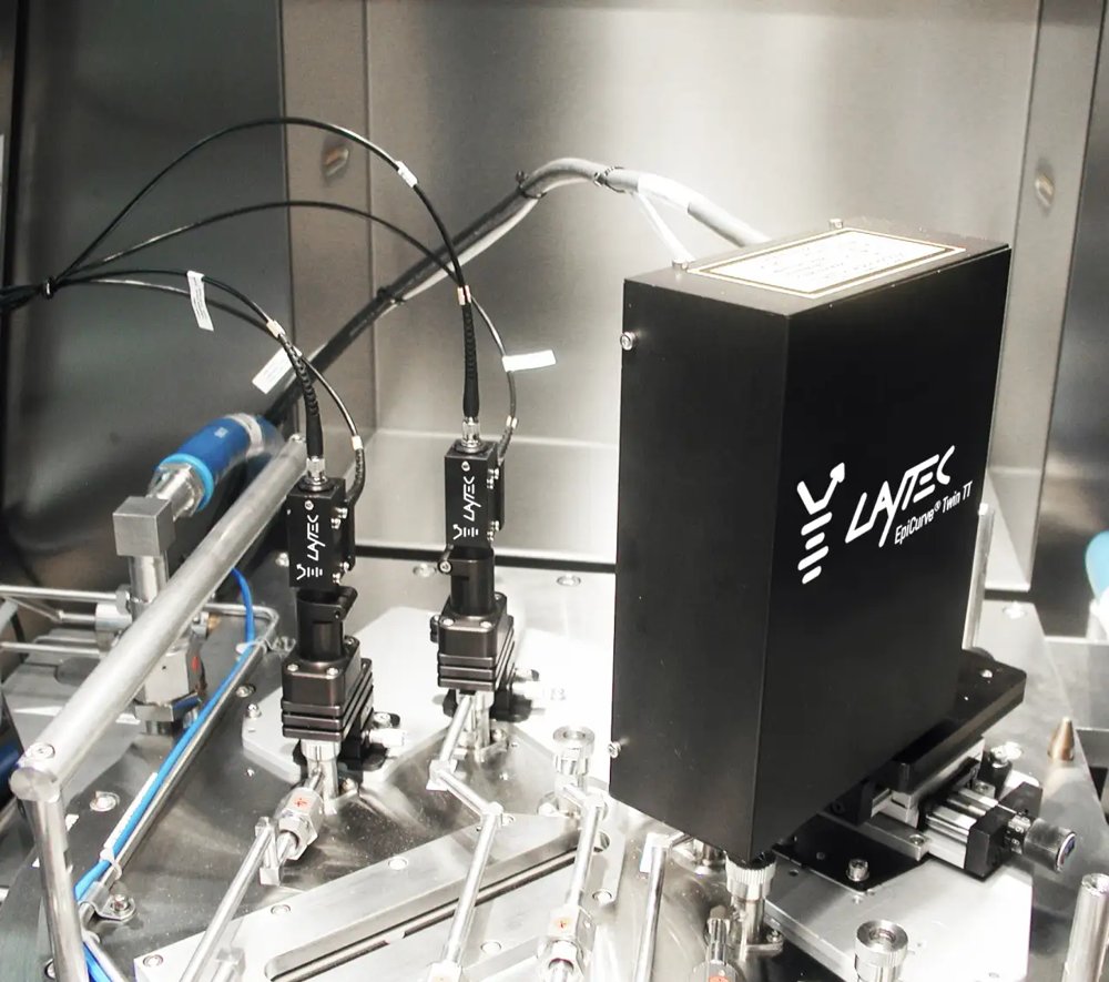
Both emissivity-corrected temperature monitoring and reflectance measurement at three wavelengths are included in all products in our EpiCurve® TT family of products. For reactors with multiple wafer ring configurations, the models with two or three EpiTT heads (EpiCurve®Twin TT and EpiCurve®Triple TT) allow for temperature and reflectance measurements at two or three independent positions respectively.
CATEGORY
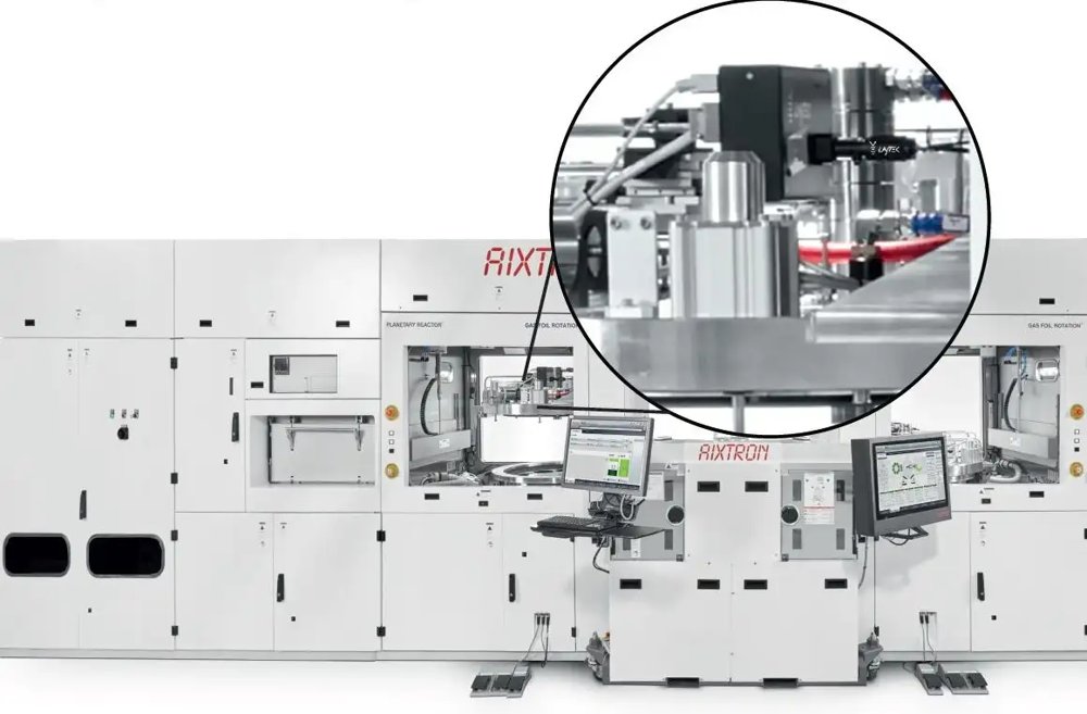
All products in the EpiTT family (EpiTT, EpiTwin TT, EpiTriple TT) are available for various MOCVD growth systems such as: - Systems with satellite rotation - Showerhead-like systems - Systems with main susceptor rotation speed up to 1500 rpm - R&D type and customized MOCVD growth systems
CATEGORY
