By AMT&C Group (Advanced Magnetic Technologies & Consulting Group)
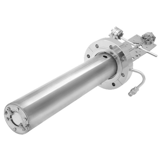
Key Systems components have patented design and include SemiTEq's technology know-how - Optical monitoring systems - Beam-flux monitor
Fast loading flanges with or without viewing window Technical characteristics - Mounting flange: 100/160/200CF
CATEGORY
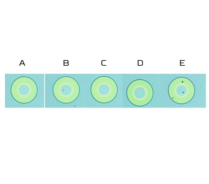
SemiTEq’s thermal processing systems are widely used for ohmic contact annealing for production of electronic devices based on A3B5 semiconductor compounds STE RTA100 systems are specially designed for short-time annealing at temperatures up to 1000°C in inert atmosphere. STE RTP150 systems enable processes at extremely high temperatures (up to 1300°C) in aggressive gases keeping high process-to-process repeatability. Precise oxidation system STE APOX75 developed in response to modern technological challenges and high customers demand for photonics and optoelectronics applications. Rapid thermal annealing - Thermal processing STA RTA100 Rapid thermal annealing system Rapid thermal processing - Thermal processing STE RTP150 Rapid thermal processing system in vacuum and controlled gas environment Precise oxidation for VCSEL - Precise oxidation STE APOX75 System for thermal oxidation of VCSEL's functional layers Technological processes - Heat uniformity measurement results on wafer Ø100 mm - Heating run-to-run reproducibility - Aperture width uniformity - Aperture depth uniformity - Heat uniformity - Ø100 mm wafer of Al203 heating at helium ambient (graphite table)
CATEGORY
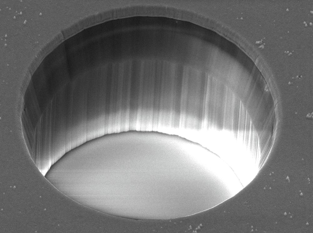
SemiTeq offers high quality solutions for plasma chemical etching and deposition systems due to many years of experience in its development, production and maintenance. We also use the results of more than 15 years of our applications experience by customers to make SemiTEq’s solutions better Versatile configuration of serial models combined with cassette loading unit or cluster connection together with wide library of basic technologies allows us to offer optimal solutions for customers technological needs. Specially developed software implements modern technological processes without adding defects into the semiconductor structure. Etching ICP-RIE STE ICP200E Plasma chemical etching system in combined capacitive and inductive discharge (ICP-RIE) RIE STE RIE200 Reactive ion etching (RIE) system Deposition ICP-CVD STE ICP200D Plasma chemical deposition system in inductively coupled plasma (ICP-CVD) PECVD STE PECVD200 Plasma enhanced chemical vapor deposition system (PECVD) Technological processes SiC deep plasma chemical etching to form metallization on the GaN transistor reverse side GaAs deep plasma chemical etching to form metallization on the GaAs transistor reverse side Si plasma chemical etching with high aspect ratio (Bosch-process) Si plasma chemical etching low wall roughness SiO2/Si plasma chemical etching with high selectivity Si plasma chemical etching Poly-Si high selectivity plasma chemical etching Mo plasma chemical etching InGaAs/AlGaAs plasma chemical etching GaAs/AlGaAs plasma chemical etching for VCSEL Si3N4 plasma chemical etching Si3N4 plasma chemical deposition on semiconductor structure with formed elements ICP-CVD
CATEGORY