By Consejo Superior de Investigaciones Científicas (CSIC)
Modular acquisition and control system with sub-nanosecond synchronisation over fibre optics. It incorporates programmable nodes, oscillator redundancy and active thermal control, ideal for high-precision and highly scalable applications. Sectors that require high-precision data acquisition—such as advanced metrology, scientific research, medical instrumentation, or distributed industrial systems—demand architectures capable of: synchronising multiple nodes with sub-nanosecond precision, maintaining temporal stability over long distances, ensuring reliability in the face of local hardware failures and environmental fluctuations, and integrating high-speed digital and analogue sensors without loss of temporal coherence. Current solutions have limitations in terms of precise synchronisation, scalability, thermal robustness, and flexibility. This new system allows these drawbacks to be overcome. A modular and distributed data acquisition and control system is presented, based on a central switch and a network of nodes interconnected by fibre optics. The solution incorporates a unique system architecture with active thermal control, and has been tested in various applications, such as modular scientific laboratory equipment. It could potentially be used in large-scale technological or medical infrastructures. This system enables high acquisition speeds, compatible with up to 1 GSPS in analogue, and operational robustness for prolonged use and critical environments. Competitive advantages: - True sub-nanosecond synchronisation. - Full scalability: allows nodes to be added without time degradation. - Very long distance fibre optic networks (>100 km) without loss of coherence, with oscillator redundancy, ensuring reliability in the event of failures. - Intelligent thermal control, ensuring stability in any operating environment. - Modular architecture, adaptable to different applications.
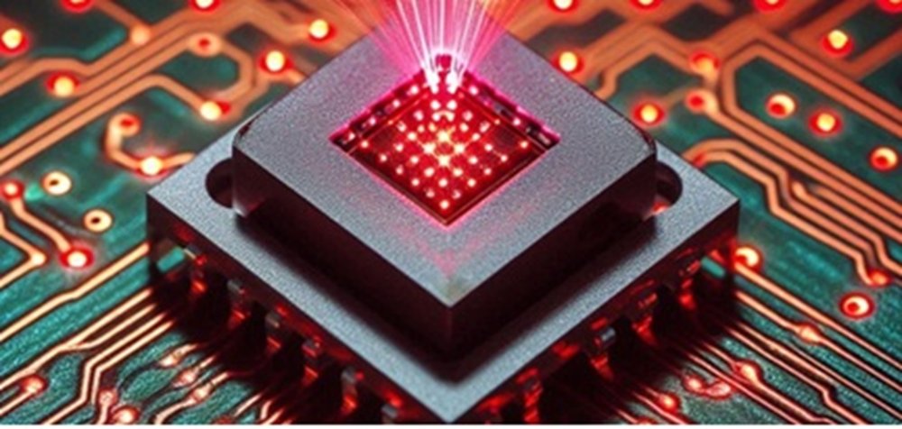
Semiconductor lasers with in-plane active layer are surface emitting devices by digging grooves into the semiconductor die. This allows to build single or multiple emitters with arbitrary shape on the same chip, with multiple frequency emission, low spatial coherence, and complex pattern beams Market need In the lighting sector, it is currently necessary to choose between intensity and incoherence. Conventional lasers, both edge-emitting and vertical cavity surface-emitting, exhibit high spatial coherence, which produces artifacts when illuminating a scene. For applications such as microscopy lighting, it is essential that lasers be diffuse cavity lasers, which have very low spatial coherence. In sectors where structured directional emission has applications, such structuring requires an additional procedure, whereas stochastic lasers provide it naturally. Proposed solution This technology leverages the discovery that diffusive surfaces enable resonant optical cavities eliminating the need for traditional mirrors in laser fabrication. Semiconductor lasers are developed with a conventional epitaxial structure, while defining the optical cavity by etching holes or grooves into the die. This design simultaneously enables optical feedback within the cavity and vertical light extraction. Competitive advantages - Industrial laser diode fabrication technology is mature. - Manufacturing can be integrated on commercial wafers. - Electrical pumping vs. optical pumping of most lasers simplifies and makes it portable. - Potential for integrated networked lasers systems. - Application in light sources with potential control on directionality, speckled spatial pattern, multi mode operation. Stage of development: TRL 3-4 Intellectual property: PCT application Intended collaboration: Licensing and/or co-development Reference: CSIC/LR/026
CATEGORY
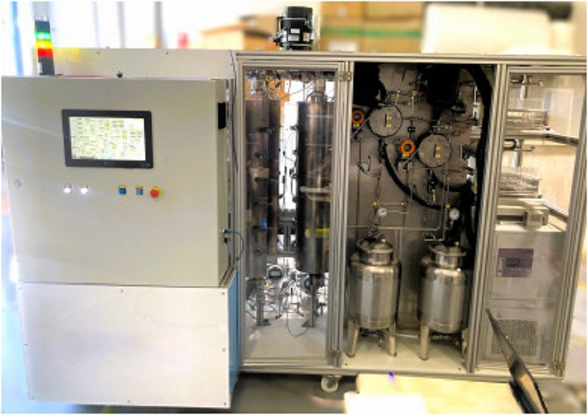
Catalyst prepared by sequential impregnation of platinum and metal oxides onto fishbone-type carbon nanofibers (CNF), enabling the production of biofuels with higher yield and superior properties compared to conventional catalysts.
CATEGORY
Rotary system that allows homogeneous ion implantation on surfaces of microstructured materials. The device avoids the shadows generated when tilting samples during the process, achieving a uniform distribution of impurities. Market need To manufacture advanced semiconductor materials, it is necessary to introduce impurities through a process called ion implantation. During this process, samples must be tilted by approximately 7 degrees to prevent ions from channelling through the crystal lattice. However, when the material surface has microstructures, this fixed tilt causes shadowing effects: parts of the sample remain hidden from the ion beam and do not receive the dopant uniformly. Current systems do not adequately solve this problem. Therefore, the market needs a device that enables uniform implantation in this type of material, thereby improving the quality of advanced semiconductors. Proposed solution A rotating system has been developed that couples to existing ion implanters. The device features a sample holder that rotates while maintaining the fixed 7-degree tilt. Rotation is transmitted from an external motor through a magnetic coupling that preserves the vacuum inside the chamber. The rotation speed is slower than the ion beam scanning speed, ensuring that the entire microstructured surface is uniformly exposed. An additional metal plate collects ions that do not impact the sample, allowing precise measurement of the implantation dose. Competitive advantages - Eliminates shadowing and guarantees uniform implantation on microstructured surfaces. - Couples to conventional ion implantation equipment without modifications. - Transmits rotation while maintaining vacuum through a sealed magnetic coupling. - Measures implantation dose in real time with an ion-collecting plate. Stage of development: Laboratory-tested prototype Intellectual property: Spanish utility model granted Intended collaboration: Licensing and/or co-development Reference: CSIC/AI/014
CATEGORY
Advanced industrial radon detection system based on an innovative cylindrical chamber design, featuring axial sensor distribution and precision focusing bars to ensure superior measurement accuracy, reliability and long-term operational stability in demanding environments. Market need Prolonged exposure to radon in confined spaces such as basements and mines poses serious health risks, including respiratory problems and lung cancer. Older and underground buildings often lack adequate ventilation, making early detection of radon essential to preserve healthy environments. Existing solutions are either very inexpensive (≈€200) but unreliable, or accurate but very costly (≈€10,000) and slow in measurement.. Proposed solution Cost-effective, high-precision, and versatile radon detection solution, designed to meet the growing market demand for monitoring in older buildings, confined spaces, and underground environments. Competitively priced compared to other reliable detection alternatives (≈€1,500), it also offers advanced features such as isotope identification and network connectivity. It consists of a cylindrical chamber with axially distributed sensors and focusing rods, providing fast, reliable, and highly accurate measurements, while offering a more affordable and precise option than existing systems. Competitive advantages - Very high sensitivity: Detects even low levels of radon quickly (minutes) and accurately, ensuring reliable monitoring in all environments at competitive cost. - ²²²Rn / ²²⁰Rn discrimination: Spectroscopic measurement, that precisely distinguishes between different radon isotopes, and other background radiation, for more accurate risk assessment. - IoT connectivity: Enables real-time data transmission and remote monitoring, making management and analysis effortless.
CATEGORY
