By LayTec GmbH
Real time control of the etching process Concept EtchNet runs on the TRIton ® control PC displaying the reflectance signals from the three LED traces – the so- called etch traces. Additionally, the plasma-intensity can also be monitored as a potential process control param - eter. The interpretation of the curves allows to identify endpoints and to control the process. For this purpose, the software can initiate start and stop signals for the respec - tive etching steps, if fully integrated in the plasma etching tool. EtchNet saves the trace reflectance data, allows an etch trace replay and endpoint recipe development and parameter modification in a recipe editor in order to adjust the recipe based on the learnings of previous runs. User interface and workflow When an operator opens the measurement view (Figure 1 ), a dual panel layout appears: reference traces on the top, live traces on the bottom. A toolbar loads ref - erence runs, links the corresponding recipe and clears or stores data. Reference runs can be derived from simula - tions, etch-through runs or previous processes, such as growth runs. Under the hood, each endpoint recipe is a sequence of logical steps – e.g. WaitForStart, Recognize Pat - tern, Delay etc. with separate parameters, shown in the editor tables underneath the color coded timeline (Figure 2 ). About a dozen step types are available to analyse the curve and react in a defined way on certain features of one or more wavelengths, again with a list of parameters. When, for example, the software sees an end - point reached, it sets the stop signal on the interface to the etching tool or prompts the operator to stop the process. The moment the user presses Run, the live window shows how the process follows the recipe. Then EtchNet logs every data point in a database. The current endpoint recipe is loaded into the hardware and executed in an automated way as soon as the endpoint has been fore - casted, detected and reached. The recorded data sets are linked to the endpoint recipe data for traceability and repeatability. For the proper positioning of the measurement spot, the spot can be moved across the wafer area in a special posi - tioning mode either based on scanning the reflectance intensity over a certain area or by employing an optional camera. During the process, the spot remains at one point on the test pad or open area. The software and the TRIton ® metrology system as a whole are designed as a toolbox system which can easily handle changes in the etch rate, the etch area or the whole etch method. Why fab engineers value EtchNet Customers from both academia and industry report three recurring gains: – Precision: endpoint detection down to sub-micron precision (depends on the etching method) is crucial for quality control. – Recipe portability: the recipe can be exported/ imported across tools or duplicated for multi chamber platforms. – Traceability: every run – raw data, recipe version, operator comments – remains searchable in the database for audits or statistical process control.
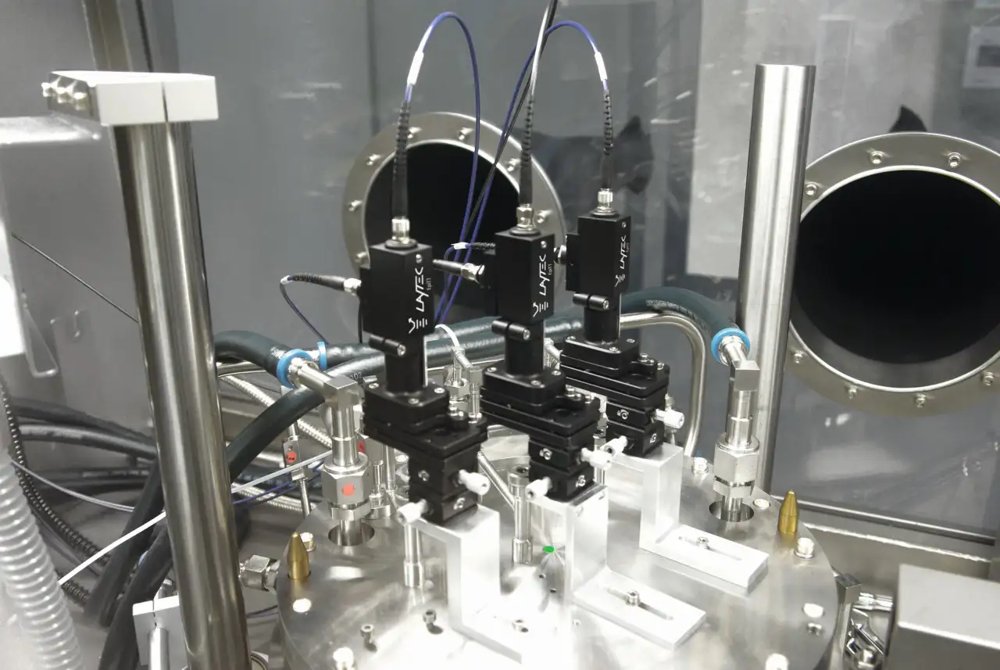
Combine measurements of temperature and reflectance at three wavelengths in one tool. EpiTT combines measurements of temperature and reflectance at three wavelengths in one tool. For True Temperature (TT), we apply the method of emissivity corrected pyrometry, which delivers the precise surface temperatures of opaque materials at 950 nm (Si, GaAs, InP). For materials that are transparent at 950 nm (GaN, Sapphire, SiC), EpiTT measures the temperature on the top side of the carrier. Measuring reflectance at three wavelengths monitors all essential properties of the growing layers, such as growth rate, film thickness, stoichiometry changes and morphology. EpiTT offers industry standard metrology for all kinds of epitaxial growth systems and is compatible with different main rotation frequencies in the range from 5-1500 rpm. Fields of application - Temperature range: T=450°C to 1300°C for large viewport systems/T=500°C to 1400°C for narrow viewport systems/other temperature ranges on request, e.g. 1500°C for UV LED applications, 1700°C for SiC - Wafer temperature with precision better than ±1K in a range of 600°C to 1400°C - Wafer and area selective measurements - True wafer temperature for opaque semiconductors such as InP, GaAs and Si - Pocket temperature for GaN, Sapphire and SiC Product features Emissivity corrected pyrometry: - Temperature range from 450°C to 1300°C for large viewport systems/500°C to 1400°C for narrow viewport systems / other temperature ranges on request, e.g. 1500°C for UV LED applications, 1700°C for SiC - Accuracy better than 1 K - Wafer and area selective measurements - True wafer temperature for opaque semiconductors such as InP, Graphite (SbS) - Pocket temperature for GaN, Sapphire and SiC Reflectance at three wavelengths: - 950 nm, 633 nm and 405 nm - Growth rate, layer thickness, roughness and other layer qualities - Full performance up to 1500 rpm main susceptor rotation - Further wavelength (e.g. 280nm, 365nm, 1550nm) for special applications are available on request
CATEGORY
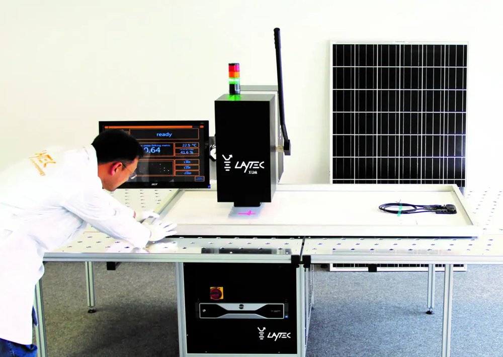
X Link® enables fast, automated, non-destructive and accurate evaluation of the level of EVA or polyolefin cross-linking in PV module encapsulation processes. In solar modules, the ethylene vinyl acetate (EVA) or polyolefin encapsulation protects the sensitive solar cells from the environment. In consequence the degree of intermolecular cross-linking of EVA or polyolefin is decisive for the long-term stability and performance of a module. Cross-linking is achieved by thermally curing the polymers during the lamination process. The X Link® system enables fast, automated, non-destructive and accurate evaluation of the level of EVA or polyolefin cross-linking immediately after lamination. It can be integrated into any solar module production site, offering a flexible platform for encapsulation quality control ranging from single point sampling to full module mapping. The stand-alone version is designed for lab applications, manual product sampling, areal mappings, R&D labs and pilot lines, ready to test full-size production-type modules with or without frames. High-resolution spatial mappings of the cross-linking degree and statistical evaluation can be performed. Furthermore, the manual off-line version allows multiple-point measurements on laminates and out-of-production modules, and modules from the field. This setup is a highly useful quality control tool for incoming goods inspection for EPCs, certifiers and consultants. Fields of application - Module encapsulation quality control in glass/backsheet solar module production Product features - Non-destructive test procedure - Testing time of only seconds per measurement points - Flexible module mapping capability - Data output in “% gel content”
CATEGORY
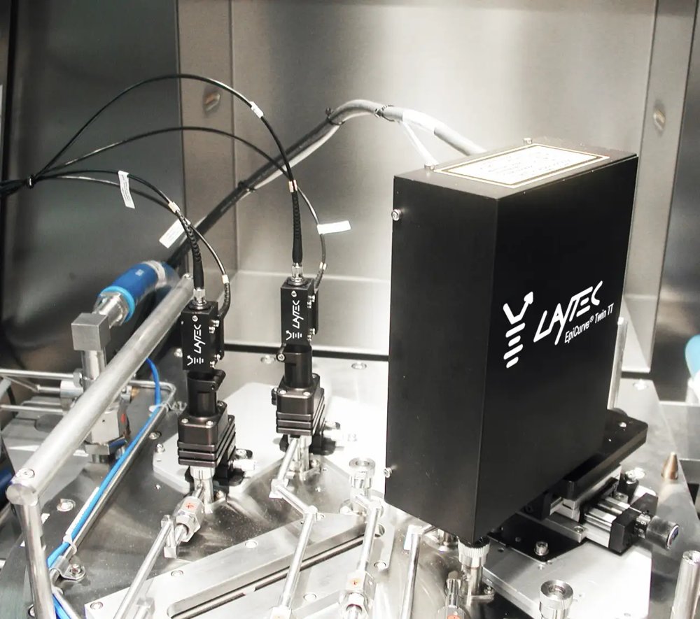
Both emissivity-corrected temperature monitoring and reflectance measurement at three wavelengths are included in all products in our EpiCurve® TT family of products. For reactors with multiple wafer ring configurations, the models with two or three EpiTT heads (EpiCurve®Twin TT and EpiCurve®Triple TT) allow for temperature and reflectance measurements at two or three independent positions respectively.
CATEGORY
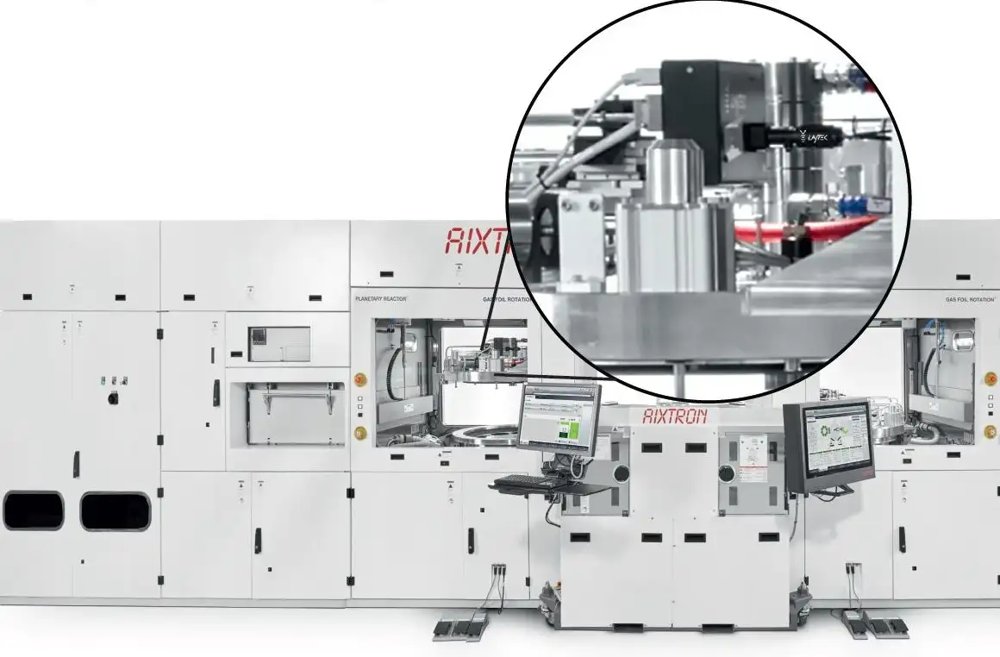
All products in the EpiTT family (EpiTT, EpiTwin TT, EpiTriple TT) are available for various MOCVD growth systems such as: - Systems with satellite rotation - Showerhead-like systems - Systems with main susceptor rotation speed up to 1500 rpm - R&D type and customized MOCVD growth systems
CATEGORY
