By EV Group
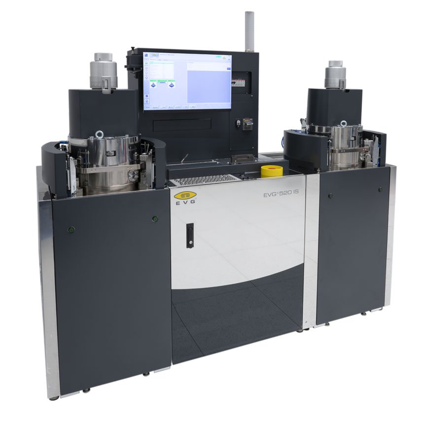
Hot Embossing Systems EV Group’s series of high-precision hot embossing systems are based on the company’s market-leading wafer bonding technology. Hot embossing is a cost-effective and flexible fabrication technology with very high replication accuracy.
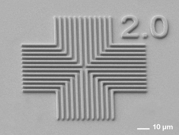
MLE (maskless exposure) technology is a revolutionary next-generation lithography technology developed by EV Group to address future back-end lithography needs for advanced packaging, MEMS, biomedical and IC substrate applications. The world’s first highly scalable maskless lithography technology for high-volume manufacturing delivers unsurpassed flexibility to enable extremely short development cycles for new devices. Heterogeneous integration is gaining more attention and is seen as a forthcoming way of achieving higher computing performances and extended device functionalities without the need for continuous scaling. The demand for the continuous innovation of the chiplet design and its integration on silicon or on package can be addressed via adaptive patterning. This new industry vision will require new high-volume manufacturing tools that can quickly integrate new designs schemes as traditional back-end lithography suffers from several limitations restricting its applicability. Moreover, continuously increasing mask costs for various layout designs and mask inventory management represents a significant part of overall development and production costs. MLE technology invented by EV Group addresses this critical demand for design flexibility, as it surmounts mask-related difficulties in both development and production phases and thus shortens development cycles. Additionally, this technology keeps your specific designs and layouts confidential as they do not need to be sent externally. This innovative ‘digital lithography’ technology bridges the gap between R&D and production while offering a scalable solution capable of dynamically addressing die and wafer-level designs simultaneously and at the same time meet critical requirements for various markets, such as advanced packaging, MEMS, biomedical and HDI PCB markets. EVG’s MLE technology enables high-resolution (<2 microns L/S), stitch-free maskless exposure of the entire substrate surface with high throughput and low cost of ownership. The system scales according to user needs – for facilitating rapid transition from R&D to HVM mode, for throughput optimization, or for adaptation to different substrate sizes and materials – and is ideal for processing a range of substrates from small silicon or compound semiconductor wafers up to panel sizes. MLE achieves the same patterning performance regardless of photoresist thanks to a flexible and scalable high-power UV laser source, which provides multiple wavelength exposure options. The aim of EVG’s novel MLE technology is not only to bring a new lithography tool to the market, but also address a critical need for smart and agile digital processing in the semiconductor industry while delivering unique maskless scalability in throughput, format and consumables-free infrastructure Features - Full-resolution, stitch-free dynamic photoresist patterning - Better than 2 µm line / space resolution in any arbitrary direction - Design freedom and data confidentiality thanks to digital programmable layouts - Individual die annotations (serial numbers, encryption keys, etc.) - Compensation of wafer level adaptive registration - Unaffected by substrate deformation and warpage (thick wafers, glass, or organic substrates) - Smart & agile digital lithography processing infrastructure - Consumables-free technology
CATEGORY
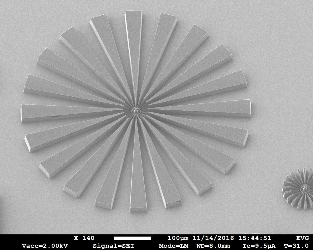
EVG’s latest enhancement for exposure optics is a UV-LED lamp house setup. LEDs have found widespread utilization in many applications due to their low-energy consumption and long lifetime. However, for many years, mercury lamps were the only light source that could provide sufficient intensity for the requirements of mask aligners. Due to recent improvements in UV-LED technology in combination with well-engineered optics, this solution even surpasses standard mercury lamps with numerous added benefits. EVG has been evaluating LED technology since 2005, bringing the world’s first functional UV-LED lamp house to the worldwide market in 2006. At that time, UV-LED technology still faced some limitations for manufacturing purposes. In 2016, EVG re-launched its UV-LED lamp house setup as UV-LED technology advanced significantly and overpassed standard mercury light source in many aspects. This technology gives its users much more flexibility for their applications in terms of UV exposure spectrum setup, as spectral lines are individually tunable and special optical filters are no longer required. Furthermore, low-energy consumption and long lifetime are among the UV-LED light source’s advantages, as no warm-up or cool-down phase is required. In addition, LEDs need to be powered only during the exposure process, and the technology eliminates the need for additional facility (exhaust, cooling gases) and lamp changes, which are regularly needed for mercury arc lamps. This ideal combination will not only minimize your running and maintenance costs but also add value with improved operator safety and environmental friendliness. Mercury and its compounds are highly toxic to humans and the environment, therefore special obligations have to be followed such as trained personnel, safety protective equipment for installation, replacements and handling, as well as storage and hazardous toxic waste disposal. The European Union is moving toward a mercury-free economy and thus issued the regulation [2017/852], which forbids production, import and export of the high-pressure mercury vapor lamps for lightning & special purposes as a first step. The United Nations addresses this environmental impact globally with the ‘Minamata Convention on Mercury’, where over 100 parties have already committed to follow this program. The latest UV-LED technology secures safe operation, meaning no risk of intoxication during the regular mercury arc lamp installation, replacements or handling. Features - Minimized operation costs - No regular lamp change requirements by qualified personal - Clean and sealed lamp house setup - Minimum facilities requirements (no exhaust or cooling) - Long life-time of the light source - Instant on/off - Spectrum lines are individually tunable - No additional costs for filters and consumables needed - No more contamination of the optics - Recipe controllable user-defined wavelength intensity settings - Green process - Mercury free - Ozone free - Low power consumption - No hazardous operation and toxic waste
CATEGORY
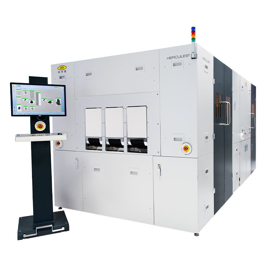
The HERCULES® is a high-volume platform integrating the entire lithography process flow in one system, reducing process footprint and operator support. Based on a modular platform, the HERCULES combines EVG’s established optical mask alignment technology with integrated wafer cleaning, resist coating, baking and resist development modules. The HERCULES enables cassette-to-cassette processing of various wafer sizes. The HERCULES safely handles thick, highly bowed, rectangular, small-diameter wafers or even device trays. Precision top-side and bottom-side alignment as well as coating of sub-micron to ultra-thick (up to 300 microns) resists can be applied for interlayer and passivation applications. The superior alignment stage design achieves highly accurate alignment and exposure results at high throughput. Features - Production platform combines all advantages of EVG’s precision alignment and resist processing systems in a minimized footprint - Versatile platform supports fully automated processing of various substrate shapes, sizes, highly warped mold wafers and even trays - Coating of up to 52,000 cP enables manufacturing of ultra-thick resist features of up to 300 microns in height - CoverSpinTM rotating cover for low resist consumption and optimized resist coating uniformity - OmniSpray®coating for optimized coating of high topography surfaces - NanoSpray®for coating and protection of via structures - Automated mask handling and storage - Optical edge exposure and/or solvent cleaning for edge bead removal - Fragile, thin or warped wafer handling of multiple wafer sizes with bridge-tool system - Rework sorting wafer management and flexible cassette system - Multi-user concept (unlimited number of user accounts and recipes, assignable access rights, different user interface languages) Technical Data Alignment modes - Top side alignment: ≤ ± 0,5 µm - Bottom side alignment: ≤ ± 1,0 µm - IR alignment: ≤ ± 2,0 µm/ substrate material depending Advanced alignment features - Manual alignment - Automatic alignment - Dynamic alignment - Alignment offset correction - Automatic cross correction / manual cross correction - Large gap alignment Industrial automation features - Cassette / SMIF / FOUP / SECS/GEM / thin, bowed, warped, edge wafer handling Exposure source - Mercury light source / UV LED light source Exposure setup - Vacuum contact / hard contact / soft contact / proximity mode / flex mode Wedge compensation - Fully automatic - SW controlled - Contactless Exposure options - Interval exposure / flood exposure / sector exposure System control - Operations system: Windows - File sharing & back-up solution / unlimited no. recipes & parameters - Multi-language user GUI & support: CN, DE, FR, IT, JP, KR - Real-time remote access, diagnostics & troubleshooting
CATEGORY
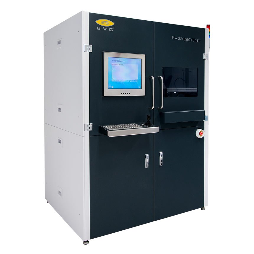
SmartNIL UV Nanoimprint Lithography System Mask alignment system with UV Nanoimprint capability featuring EVG´s proprietary SmartNIL® technology up to 150 mm Known for its automation flexibility and reliability, this system provides state-of-the-art mask alignment technology on a minimized footprint. Operator-friendly software, minimized time for mask and tooling changes, as well as efficient worldwide service and support makes it the ideal solution for any R&D environment up to semi-automated volume production. The tool supports a variety of standard lithography processes, such as vacuum-, soft-, hard- and proximity exposure mode. Furthermore, the EVG’s proprietary SmartNIL technology is supported. SmartNIL is the industry-leading NIL technology, enabling the patterning of extremely small features down to less than 40 nm, as well as a wide range of structure sizes and shapes. SmartNIL in combination with multi-use soft-stamp technology enables unmatched throughput with considerable cost-of-ownership advantages while preserving scalability and maintenance-friendly operation. EVG’s SmartNIL redeems the long-term promise of nanoimprinting being a low-cost and high-volume alternative lithography technology for mass manufacturing of micro- and nanoscale structures. resolution dependent on process and template Features - Top-side and bottom-side alignment capability - High-precision alignment stage - Automated wedge compensation sequence - Motorized and recipe controlled exposure gap - Supports the latest UV-LED technology - Minimized system footprint and facility requirements - Step-by-step process guidance - Remote tech support - Multi-user concept (unlimited number of user accounts and recipes, assignable access rights, different user interface languages) - Agile processing and conversion re-tooling - Table top or stand-alone version with anti-vibration granite table - Additional capabilities: - Bond alignment - IR alignment - Smart NIL® - µ-contact printing Technical Data Wafer diameter (substrate size) Standard lithography: 75 up to 200 mm Soft UV-NIL: 75 up to 200 mm SmartNIL®: up to 150 mm Resolution ≤ 40 nm (resolution dependent upon template and process) Supported Process Soft UV-NIL & SmartNIL® Exposure source Mercury light source or UV LED light source Alignment Soft-NIL: ≤ ± 2 µm SmartNIL®: ≤ ± 3 µm Automated separation Soft UV NIL: not supported SmartNIL®: supported Working stamp fabrication Soft UV-NIL: external SmartNIL®: supported
CATEGORY
