Nanomembrane-enabled barrier devices for cell culture Product Nos. GASKET-MW Provided Kit Materials - Pre-Cut Polydimethyl Silicone (PDMS) Gasket Set (suitable for 10 devices) Required Equipment & Supplies Equipment - UV Ozone generator or Oxygen Plasma Oven - Hot Plate or gravity oven Supplies - Tweezers suitable for membrane manipulation (SiMPore K6TWZR, or equivalent) - User-supplied 24-well pre-sterilized Microplate - Tray or substrate suitable for plasma or UV ozone activation - Alcohol wipes or KimWipe saturated with an alcohol solution (70%) - Absolute Alcohol (such as Isopropyl Alcohol (IPA) or Ethanol) - Culture media (lab prepared or user supplied) - Gloves and other suitable personal protective equipment (PPE) Gasket Stack Layout Layer # Material 1 (Basal Well Layer) 1600 μm platinum cured PDMS 2 (Membrane Chip) 300 μm SiN/Si membrane chip 3 (Apical Well Layer) 1600 μm platinum cured PDMS Instructions For Use: MultiWell Plate Development Kit. SiMPore membranes are deposed across the surface of a silicon wafer support material. Access to the membrane is achieve by etching trenches through the silicon wafer support, yielding the cross-sectional geometry shown above. Device Fill Volumes Well Max Volume (μL) Recommended Volume (μL) Apical 22.5 20 Basal 50 45 PHYSICAL PROPERTIES Membrane Composition: Silicon Nitride (SiN) Membrane Surface Area 1.4 mm2 (single slot), 6.3 mm2 (three slot) Minimum Working Length 2000 μm Membrane Thickness: 100 nm (NPN) / 400 nm (SiN) Pore Size Cut-Off: varies Porosity: varies Surface Charge: Neutral to slightly negative Wetted Components Material(s): PDMS, Si, SiN, SS, PC/PS (MultiWell Plate) SPECIFICATIONS Sterilization MultiWell devices may be sterilized via Ethylene Oxide, Hydrogen Peroxide Gas, 70% IPA immersion, or gamma, UV, and E-Beam irradiation after removing from the plastic bag. Do Not Sterilize via steam autoclave as device damage may occur. Chemical Stability Devices are incompatible with strong bases, as membrane degradation may occur. Avoid long exposure durations to solvents, as this may compromise device integrity. Do not apply solvents, acids, bases, organics, or other compounds that are incompatible with the stated device components. Device Storage Store in a clean and dry environment. Prolonged exposure to UV can degrade the PDMS bonding, leading to poor layer adhesion and shortened service life. STANDARD WARRANTY SiMPore Inc. (“SiMPore”) warrants its products will meet their applicable published specifications when used in accordance with their applicable instructions for a period of one year from shipment of the products.
Pure silicon grids offer greater stability at high beam currents and at moderately high annealing temperatures (up to 600°C). Increases stability Enables alternative for elemental analysis Pure silicon grids enable elemental analyses by EDAX and EELS of samples containing nitrogen and/or carbon due to their composition and their minimal background signal. Reduces chromatic blur Compared to carbon grids, pure silicon grids have half the chromatic blur. 15 nm thick Pure Silicon TEM Grids are our most robust pure silicon films; these amorphous films offer plasma cleanability, tunable surface hydrophobicity, and the ability to analyze for nitrogen and carbon without background signals Our 5nm amorphous silicon TEM windows are less prone to elastic scattering than alternative technologies Long two slot 50 X 1500 micron windows enable high angle electron tomography imaging
CATEGORY
Silicon nitride grids are well-suited for use in environmental TEMs where dynamic processes are observed at high temperatures. Ideal for temperatures 1000°C Flat and uniform surface Silicon nitride grids incorporate LPCVD, low-stress (~250MPa), non-stoichiometric silicon nitride which provides uniformly flat, insulating, and hydrophobic surfaces. Made for stable imaging Nanoporous and microporous silicon nitride grids support stable suspension of nanoscale materials for imaging without a background. Microporous and nanoporous silicon nitride permit free suspension of deposited material for background-free imaging 10, 20 & 50 nm thick Silicon Nitride TEM Grids are our most robust, flat, and plasma cleanable substrates for demanding sample preparation procedures
CATEGORY

Our Electron X-Ray microscopy windows are available with freestanding silicon nitride or G-FLAT® silicon dioxide membranes in a range of window sizes and membrane thicknesses for various vacuum and temperature conditions. Our 500 x 500 micron silicon nitride membranes with 50 nm and 100 nm thick single windows withstand full vacuum differential pressure and permit high X-Ray transmission across a wide spectrum. Our 1,500 x 1,500 micron and 2,500 x 2,500 micron silicon nitride membranes offer large imaging areas and high X-Ray transmission and are compatible with partial vacuum conditions. State-of-the-art manufacturing processes and an expert engineering team allow us to offer all variations of our X-Ray Windows at competitive prices. Unlike our competitors, all our X-Ray Electron Microscopy products are made entirely in the USA. Incredibly durable Low-stress LPCVD Silicon Nitride membranes are mechanically strong and well-suited for high temperature and differential pressure environments. Plasma cleanable All of our X-Ray Windows can be vigorously plasma cleaned to remove organic contamination. Increases uniformity Flat, uniformly deposited films provide consistent backgrounds with low field-to-field variability and high X-Ray transmission.
CATEGORY
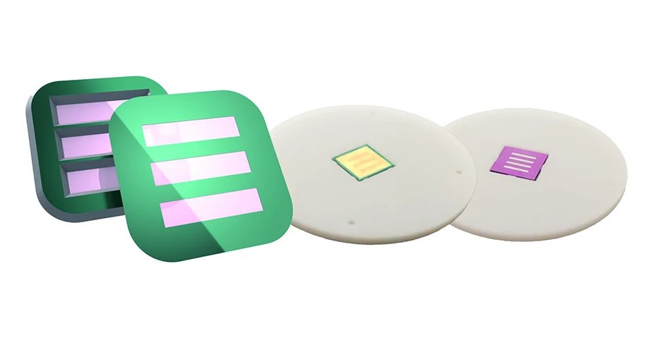
Research findings indicate that viral particles prepared on Cryo-SiN exhibit greater contrast in comparison to those prepared on holey carbon films under the same conditions. Greater contrast Less imaging It is significantly easier to calculate 3D reconstructions of viral particles when they’re prepared on Cryo-SiN, as they require only a fraction of the images required for samples prepared on holey carbon films. Our Cryo EM grids include Silicon Nitride alone or with unique carbon coatings to provide superior bridging and maximum observable specimen sites of organic and biologic solutions and suspensions.
CATEGORY
