By SAMCO Inc.
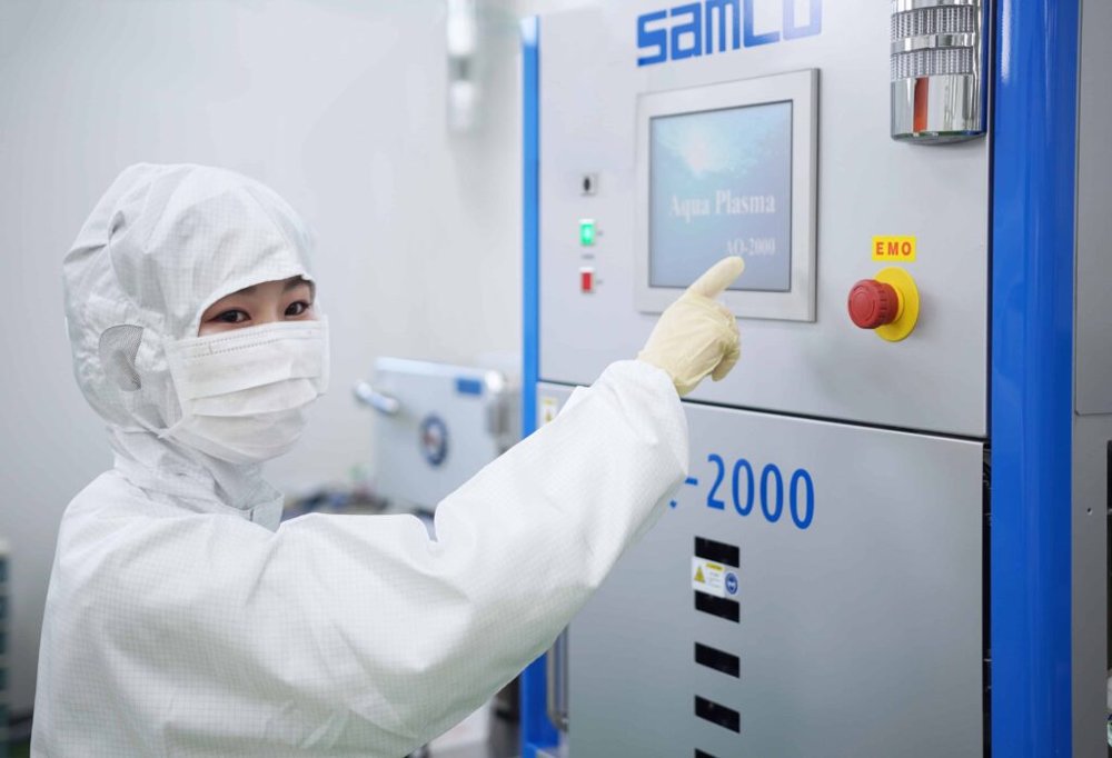
Samco’s Surface Treatment Systems provide comprehensive cleaning solutions tailored to ensure the highest quality and consistency in surface preparation. Using advanced plasma and UV ozone techniques, these systems remove organic and inorganic contaminants, enabling optimal adhesion and performance of films and coatings. Our Aqua Plasma® Cleaners leverage environmentally friendly water vapor plasma to reduce oxides, remove organic residues, and enhance hydrophilic properties. Plasma Cleaning Systems offer flexible batch processing for various materials and applications, from R&D to large-scale production. For substrates requiring gentle, residue-free treatment, our UV Ozone Cleaning Systems utilize a combination of UV light, ozone, and stage heating, providing thorough cleaning for materials like silicon, glass, and compound semiconductors.
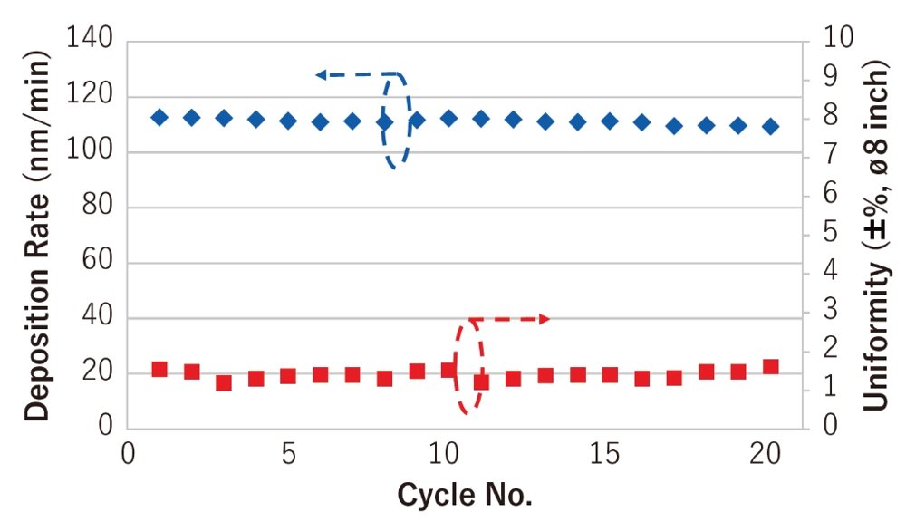
Figure 1 shows the overall appearance of the PD-2201HLC. The system consists of a cassette chamber capable of accommodating both tray cassettes and wafer cassettes, a load-lock chamber, and a reaction chamber. In addition, the system can be equipped with an optional remote plasma cleaning function and offers expandability for additional reaction chambers. To improve productivity, enhancements were made to the heater structure, electrode design, and cleaning functionality. In the previous model, heater ramp-up and cool-down times had a significant impact on cycle time. To address this issue, the PD-2201HLC employs a newly developed heater with excellent heat resistance and corrosion resistance. This enables shorter heating and cooling times, thereby reducing waiting time between processes. Next, the electrode structure was optimized to improve within-wafer thickness uniformity during high-rate deposition. Figure 2 compares the deposition rate, within-wafer uniformity, and stress control of the previous model and the PD-2201HLC as a function of RF power density. In the previous model, although within-wafer uniformity was excellent, increasing the deposition rate was challenging. Increasing process parameters such as RF power and pressure raised the deposition rate, but also changed the plasma characteristics, which tended to degrade within-wafer uniformity and stress control (Figure 2(a), (b)). To overcome this limitation, the electrode structure of the PD-2201HLC was optimized to achieve a more uniform plasma distribution. As a result, the PD-2201HLC enables high deposition rates while maintaining within-wafer uniformity and stress control at levels comparable to those of the previous model (Figure 2(c), (d)). Finally, the addition of an optional remote plasma cleaning function significantly reduces reaction chamber cleaning time. This reduces non-deposition process time and contributes to improved overall equipment utilization. Figure 3 compares the takt time of the previous model and the PD-2201HLC. Through the combination of shorter heating and cooling times enabled by the new heater, support for high-rate deposition through optimized electrode design, and reduced cleaning time through remote plasma cleaning, the time required per cycle was reduced by approximately 70% compared with the previous model. Figure 4 shows the repeatability results for SiN film deposition using the PD-2201HLC. Following a single pre-coating process of 1 µm, ten batches of 500 nm SiN deposition were performed, followed by chamber cleaning. This sequence was defined as one cycle. A total of 20 consecutive cycles were conducted, and the deposition rate and within-wafer thickness uniformity of Ø8-inch SiN films were evaluated. Over the 20 deposition cycles, virtually no variation was observed in the deposition rate or within-wafer uniformity, confirming that stable deposition performance can be maintained. This report introduced the new plasma CVD system, “PD-2201HLC,” developed with the aim of improving productivity. This system achieves reduced heating and cooling times through the adoption of a new heater, improved within-wafer uniformity of film thickness during high-speed deposition through optimized electrode spacing, and reduced cleaning time via a remote plasma cleaning function. Through these improvements, the PD-2201HLC reduces the takt time per cycle by approximately 70% compared with the previous model, while maintaining high deposition rates and excellent within-wafer uniformity. Furthermore, repeatability evaluations confirmed that both the deposition rate and within-wafer uniformity remain stable throughout continuous operation.
CATEGORY
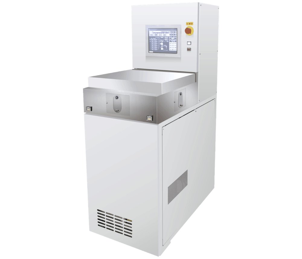
⌀220 mm Open Load Low-cost and high-performance The RIE-10NR is a novel low-cost, high-performance, fully automatic reactive ion etching system which meets the most demanding process requirements for non-corrosive gas chemistry. A computerized touch screen provides a user-friendly interface for parameter control and storage. The system enables accurate sidewall profile control and high etch selectivity between materials. With its sleek, compact design, the RIE-10NR requires minimal cleanroom space. Key Features & Benefits - Processing up to ø220 mm (ø3” x 5, ø4” x 3, ø8” x 1) - Highly selective anisotropic etching meets demanding process requirements - Fully automatic “one-button” operation with full manual override - A computerized touch screen provides a user-friendly interface for parameter control and storage - Automatic pressure control that allows for precise control of process pressure independent of gas flow - Dry pump and system layout allow for ease of maintenance - The reliable and durable system with a global installed base of more than 400 systems Applications - Etching of various materials such as Si, SiO2, SiN, Poly-Si, GaAs, Mo, Pt, Polyimide, etc. - Selective layer etching in failure analysis - Photoresist ashing, stripping, and descuming - Surface modification (wettability and adhesion improvement) Processes Failure Analysis RIE plasma etching of SiO2 Papers Paper 1: Mohammed Ashraf, Sree V. Sundararajan, Gianluca Grenci, “Low-power, low-pressure reactive-ion etching process for silicon etching with vertical and smooth walls for mechanobiology application,” J. Micro/Nanolith. MEMS MOEMS 16(3) 034501 (10 July 2017) https://doi.org/10.1117/1.JMM.16.3.034501 Paper 2: Hashimoto, S. “Micro Machined Slit Between Ridge and Groove in Micro Fluid-Channel to Measure Floating Cell Deformability.” Proceedings of the ASME 2020 Fluids Engineering Division Summer Meeting collocated with the ASME 2020 Heat Transfer Summer Conference and the ASME 2020 18th International Conference on Nanochannels, Microchannels, and Minichannels. Volume 3: Computational Fluid Dynamics; Micro and Nano Fluid Dynamics. Virtual, Online. July 13–15, 2020. V003T06A004. ASME. https://doi.org/10.1115/FEDSM2020-20073
CATEGORY
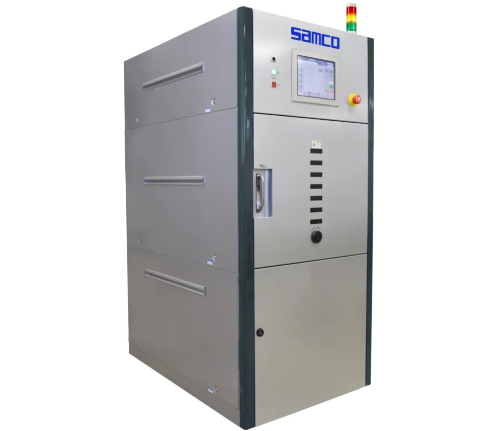
Samco’s Plasma Cleaners are parallel-plate systems capable of cleaning organic and inorganic contamination from the surface of samples. The process chamber allows the user to install multiple electrode shelves, and the flexibility of the shelf electrode configuration supports batch processing of a wide range of products, from research to high volume production. Samco plasma cleaners are trusted by R&D and mass production customers worldwide for their reliability and performance. Designed with a compact footprint, these systems enable efficient batch processing using adjustable multiple shelves, making them versatile for a wide range of applications. The PC-300 and PC-2000 models are plasma cleaning systems utilizing parallel-plate direct plasma technology. These systems effectively remove organic and inorganic contaminants from various surfaces, including plastic packages, LCD substrates, multi-chip modules, and hybrid ICs. Additional applications include photoresist ashing, ink removal, surface activation, and wettability improvement. Key advantages of Samco plasma cleaners include: - Flexible configurations: Adjustable chamber shelves accommodate both small electronic components and larger substrates. - Batch processing: Simultaneously clean multiple samples to enhance throughput and efficiency. - Versatile applications: Suitable for a range of processes, from contaminant removal to surface treatment. - Broad material compatibility: Designed for use with diverse materials, such as plastic packages, LCD substrates, and hybrid ICs. - User-friendly operation: Fully automated systems with an intuitive touchscreen interface for ease of use. - Reliable cleaning technology: Parallel-plate direct plasma ensures consistent, precise, and high-quality cleaning. With their robust capabilities and user-centric design, Samco plasma cleaners are an ideal solution for diverse cleaning and surface treatment needs. Applications - Surface cleaning of plastic packages and leadframes - Precision cleaning of optical components and molds - Surface modification (wettability and adhesion improvement) - Photoresist ashing, stripping, and descuming - Removal of organic contaminants
CATEGORY
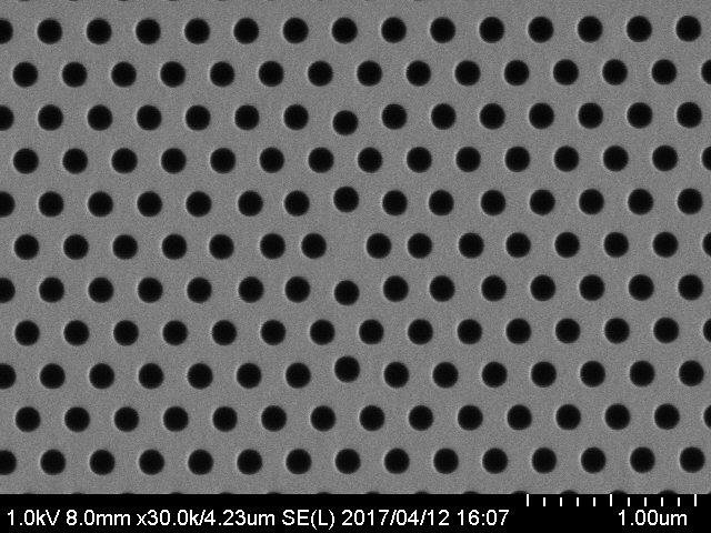
Compact model for R&D The RIE-400iP, a load lock ICP-RIE plasma etching system, utilizes high-density inductively coupled plasma (ICP) to achieve precise etching. Designed for wafers up to 100 mm (4 inch), the system features an advanced ICP source, temperature-controlled electrode, and a high-flow exhaust system, all within a compact, space-saving design. This system provides reliable and exceptional process control, ensuring excellent efficiency for a wide range of etching applications, including GaN, GaAs, InP, SiC, and various other materials. ⌀4″ Load Lock HSTC™ none Key Features & Benefits - Advanced ICP source enables highly uniform, high selectivity, and precise etching - 2 kW RF power can be applied efficiently and stably - ESC and He backside cooling for optimum temperature control - The high flow exhaust system directly connected to the reaction chamber - Compatible with ø2″, 3″, and 4″ wafers - In-situ end-pointing using interferometric and/or optical emission spectroscopic endpoint monitors - Fast-switching gas input for ALE process as an option Applications - InP ridge etch for edge emitting laser - InP DFB grating etch - GaAs/AlGaAs mesa etch for VCSELs - High selectivity etch of GaN/AlGaN - GaN recess etch - SiC/GaN trench etch for power electronics - GaSb/InSb etch for NIR/SWIR sensors - SiO2 and SiNx etch - Al, Cr, Ni etch Options - Interferometric endpoint monitor - Optical emission spectroscopy (OES) endpoint monitor - Fast-switching gas line for ALE process
CATEGORY
