By one-graphene
After a decade of CVD graphene, we have curated a perfect blend of top-notch CVD graphene films for innovation, research, and applications! This range of single-crystalline CVD graphene films and transfer services is meticulously crafted to deliver unparalleled performance. We've left no stone unturned in bringing this one-of-a-kind two-dimensional material for your scientific pursuits and satiating the world’s technological thirst for technology and innovation.
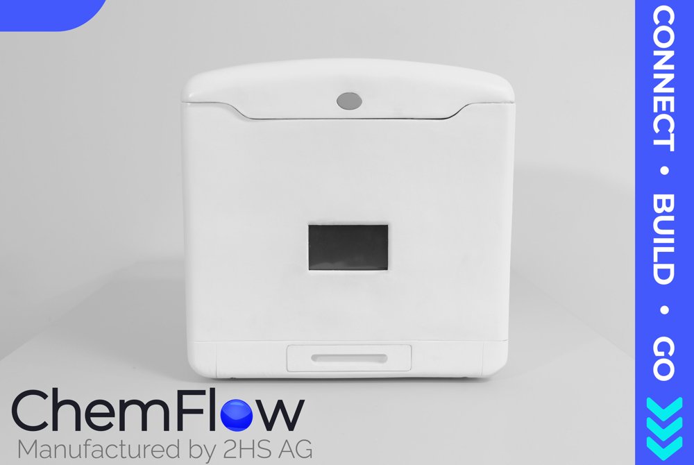
Automate Your Chemical Process Flow with Total Precision Full control over timing, volume, and sequence — in a compact system purpose-built for cleanroom environments and R&D laboratories. Cleanroom Processing Bio-Sample Dissolution 2D Material Integration Launching 2026 — Pre-orders Open CONNECT BUILD GO Low Labour Cost Improved Process Reproducibility Faster Recipe Qualification Less Chemical Waste ISO 5 Cleanroom Compatible Academic & Industrial Cleanroom Processing: Automate wet-bench chemistry while maintaining ISO 5 compliance. Eliminate operator variability across etching, cleaning, and development processes with programmable, sealed chemical handling. Photoresist develop & strip sequences RCA & Piranha wafer cleaning Buffered HF oxide etching Solvent rinse cascades Metal lift-off processing Acid Digestion for Bio-Sample Analysis: Streamline sample dissolution workflows for ICP-MS, ICP-OES, and AAS analysis. Control acid volumes, dwell times, and addition sequences to achieve complete digestion with minimal reagent use. HNO₃/HCl sequential acid digestion Tissue & environmental matrix dissolution Trace metal extraction workflows Multi-element pre-concentration Reproducible 2D Material Processing: Achieve consistent 2D material integration and processing with programmable etchant exposure, precise rinse cycles, and controlled drying — eliminating the variability of manual wet transfer. PMMA-assisted graphene transfer Copper foil etchant cycling (FeCl₃/APS) DI water rinse & float sequences MoS₂ & hBN layer processing Polymer scaffold removal Process Reproducibility: Manual - Operator-dependent; ChemFlow Pro - ±0.01 mL accuracy Timing Precision: Manual - Stopwatch + judgment; ChemFlow Pro - Programmable to ±0.1s Hands-On Time / Run: Manual - 45–90 min active; ChemFlow Pro - <5 min setup Unattended Runs: Manual - Not possible; ChemFlow Pro - 24/7 operation Recipe Recall: Manual - Re-read protocol each time; ChemFlow Pro - One-tap recall Operator Safety: Manual - Prolonged chemical exposure; ChemFlow Pro - Sealed processing Chemical Waste: Manual - High — overuse common; ChemFlow Pro - ~40% reduction Data Logging: Manual - Manual notebook; ChemFlow Pro - Auto-logged reports Connect & Configure: Plug in power and connect reservoirs. The touchscreen guides you through initial calibration in under 10 minutes. Build Your Recipe: Define each process step with precise volumes, timing, and temperatures. Save recipes for instant recall across your team. Load & Start: Place your sample, select the recipe, and press start. The system handles dispensing, timing, and sequencing automatically. Review & Export: Access complete process logs, analytics, and reports. Export data via USB, network, or direct to your LIMS. Pre-validated compatible: HCl HNO₃ H₂SO₄ H₃PO₄ Acetic acid NaOH KOH NH₄OH H₂O₂ (30%) Acetone IPA Methanol Ethanol NMP DMSO DI Water FeCl₃ APS (ammonium persulfate) KI/I₂ Developer (AZ/MF series) SC-1 / SC-2 mixtures Consult before use: HF (buffered), HF (conc.) — consult, TMAH, H₂O₂ (50%+) — consult, Piranha solution, Chromium etchants — consult
CATEGORY
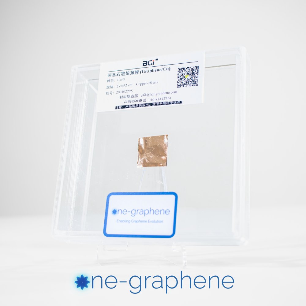
Single crystalline CVD graphene film synthesized on single crystalline copper foil (Cu 111). Size: 2 cm x 2 cm Thickness: ~20-50 micrometer Coverage: 99% Monolayer: 95% Crystal orientation: Cu<111
CATEGORY
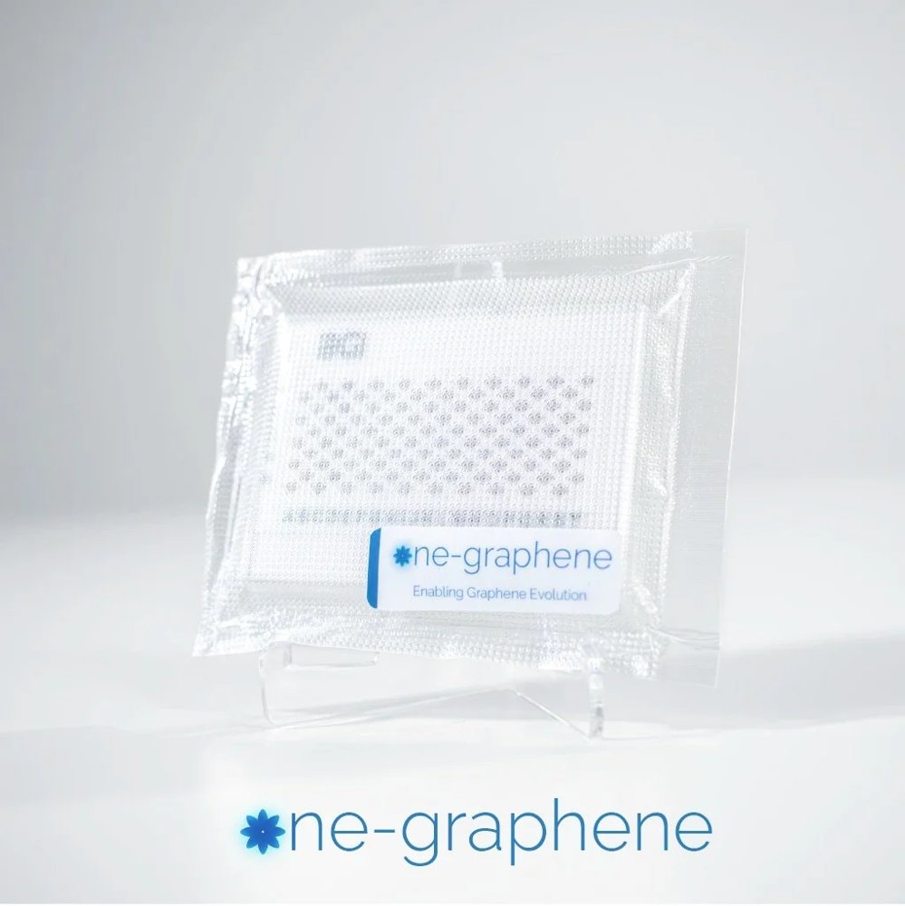
Low roughness Single-crystalline CVD graphene TEM Grids for Low-Noise Electron Microscopy Imaging Grid Material: Gold Size: 3 mm diameter Thickness: 25 micrometer Total: 20 grids
CATEGORY
Graphene Film - Single-Crystal (Cu-S Series) Growth Method Cu synthesis on single crystallized Cu Appearance Transparent Transparency 97% Coverage 99% Monolayer Rate 95% Sheet Resistance on SiO2/Si Substrate 300-400 Ω/sq Quality Control before Deliver Raman & Optical Microscopy checked Substrate - Cu Foil Thickness 20-50 μm Treatment single crystallized Cu foil Crystal Orientation Cu(111) Product Size (cm2) 2x2 5x5 10 x10
CATEGORY
